Touch-sensitive artificial skin lets robots feel and touch objects
September 13, 2010

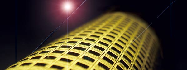
E-skin device with nanowire active matrix circuitry. Each dark square represents a single pixel. (Ali Javey and Kuniharu Takei, UC Berkeley)
Engineers at UC Berkeley have developed “e-skin,” a pressure-sensitive electronic material from semiconductor nanowires that functions like the human skin, which means incorporating the ability to feel and touch objects.
A touch-sensitive artificial skin would help overcome a key challenge in robotics: adapting the amount of force needed to hold and manipulate a wide range of objects.
A longer term goal would be to use the e-skin to restore the sense of touch to patients with prosthetic limbs, which would require significant advances in the integration of electronic sensors with the human nervous system.

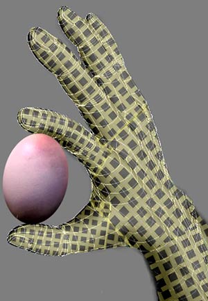
An artist’s illustration of an artificial e-skin with nanowire active matrix circuitry covering a hand. The fragile egg illustrates the functionality of the e-skin device for prosthetic and robotic applications.
Previous attempts to develop an artificial skin relied upon organic materials because they are flexible and easier to process. The problem is that organic materials are poor semiconductors, which means electronic devices made out of them would often require high voltages to operate the circuitry,” said Ali Javey, associate professor of electrical engineering and computer sciences and head of the UC Berkeley research team developing the artificial skin.
“Inorganic materials, such as crystalline silicon, on the other hand, have excellent electrical properties and can operate on low power. They are also more chemically stable. But historically, they have been inflexible and easy to crack. In this regard, works by various groups, including ours, have recently shown that miniaturized strips or wires of inorganics can be made highly flexible — ideal for high performance, mechanically bendable electronics and sensors.”
The UC Berkeley engineers utilized an innovative fabrication technique that works somewhat like a lint roller in reverse. Instead of picking up fibers, nanowire “hairs” are deposited.
The researchers started by growing the germanium/silicon nanowires on a cylindrical drum, which was then rolled onto a sticky substrate. The substrate used was a polyimide film, but the researchers said the technique can work with a variety of materials, including other plastics, paper or glass. As the drum rolled, the nanowires were deposited, or “printed,” onto the substrate in an orderly fashion, forming the basis from which thin, flexible sheets of electronic materials could be built.
In another complementary approach utilized by the researchers, the nanowires were first grown on a flat source substrate, and then transferred to the polyimide film by a direction-rubbing process.
For the e-skin, the engineers printed the nanowires onto an 18-by-19 pixel square matrix measuring 7 centimeters on each side. Each pixel contained a transistor made up of hundreds of semiconductor nanowires. Nanowire transistors were then integrated with a pressure sensitive rubber on top to provide the sensing functionality. The matrix required less than 5 volts of power to operate and maintained its robustness after being subjected to more than 2,000 bending cycles.
The researchers demonstrated the ability of the e-skin to detect pressure from 0 to 15 kilopascals, a range comparable to the force used for such daily activities as typing on a keyboard or holding an object. In a nod to their home institution, the researchers successfully mapped out the letter C in Cal.
“This is the first truly macroscale integration of ordered nanowire materials for a functional system — in this case, an electronic skin,” said study lead author Kuniharu Takei, post-doctoral fellow in electrical engineering and computer sciences. “It’s a technique that can be potentially scaled up. The limit now to the size of the e-skin we developed is the size of the processing tools we are using.”
Reference: Nanowire active-matrix circuitry for low-voltage macroscale artificial skin
More info: UC Berkeley news