A first: Stanford engineers build basic computer using carbon nanotubes
September 26, 2013

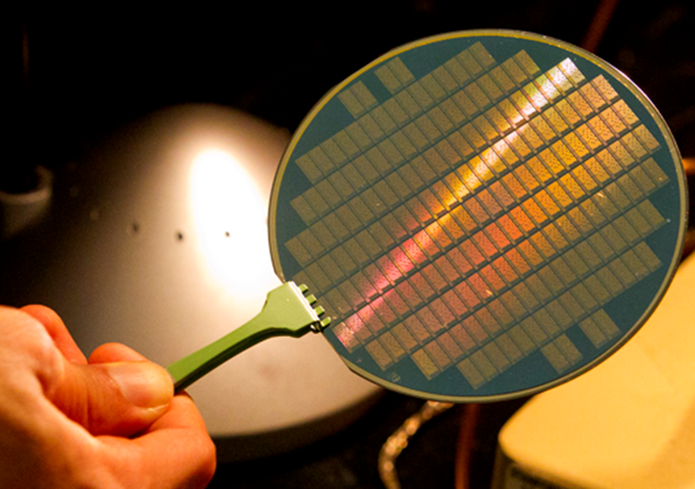
This wafer contains multiple tiny computers using carbon nanotubes (credit: Norbert von der Groeben)
A team of Stanford engineers has built a basic computer using carbon nanotubes (CNTs) — a semiconductor material with the potential to launch a new generation of smaller electronic devices that run faster, while using less energy, than those made from silicon chips.
This unprecedented feat culminates years of efforts by scientists around the world to harness this promising but quirky material.
The achievement is reported today in an article on the cover of the journal Nature written by Max Shulaker and other doctoral students in electrical engineering. The research was led by Stanford professors Subhasish Mitra and H.-S. Philip Wong.
“People have been talking about a new era of carbon nanotube electronics moving beyond silicon,” said Mitra, an electrical engineer and computer scientist. “But there have been few demonstrations of complete digital systems using this exciting technology. Here is the proof.”

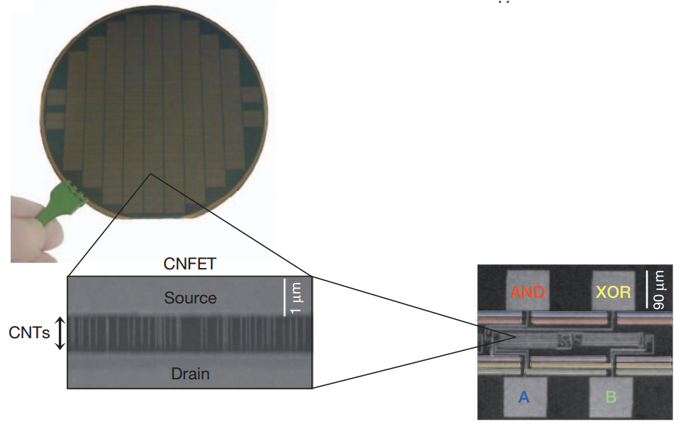
A scanning electron microscopy image of a section of the first-ever carbon nanotube computer (credit: Butch Colyear)
Mihail Roco, a senior advisor for nanotechnology at the National Science Foundation, called the Stanford work “an important scientific breakthrough.”
Professor Giovanni De Micheli, director of the Institute of Electrical Engineering at École Polytechnique Fédérale de Lausanne in Switzerland, highlighted two key contributions the Stanford team has made to this worldwide effort.
“First, they put in place a process for fabricating CNT-based circuits,” De Micheli said. “Second, they built a simple but effective circuit that shows that computation is doable using CNTs.”
He called the Stanford work “a major benchmark” in moving CNTs toward practical use.
CNTs are long chains of carbon atoms that are extremely efficient at conducting and controlling electricity. They are so thin – thousands of CNTs could fit side by side in a human hair – that it takes very little energy to switch them off, according to Wong, a co-author of the paper.
“Think of it as stepping on a garden hose,” Wong said. “The thinner the hose, the easier it is to shut off the flow.”
In theory, this combination of efficient conductivity and low-power switching make carbon nanotubes excellent candidates to serve as electronic transistors.
“CNTs could take us at least an order of magnitude in performance beyond where you can project silicon could take us,” Wong said.
Carbon nanotubes were first fashioned into transistors, the on-off switches at the heart of digital electronic systems, roughly 15 years ago. But a bedeviling array of imperfections in these carbon nanotubes has long frustrated efforts to build complex circuits using CNTs:
- CNTs do not necessarily grow in neat parallel lines, as chipmakers would like. Over time, researchers have devised tricks to grow 99.5 percent of CNTs in straight lines. But with billions of nanotubes on a chip, even a tiny degree of misaligned tubes could cause errors, so that problem remained.
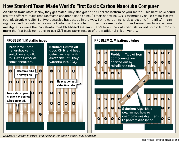
- Depending on how the CNTs grow, a fraction of these carbon nanotubes can end up behaving like metallic wires that always conduct electricity, instead of acting like semiconductors that can be switched off.
Since mass production is the eventual goal, researchers had to find ways to deal with misaligned and/or metallic CNTs without having to hunt for them like needles in a haystack.
“We needed a way to design circuits without having to look for imperfections or even know where they were,” Mitra said.
How the first carbon nanotube computer was made
The Stanford paper in Nature describes a two-pronged approach that the authors call an “imperfection-immune design.”
- To eliminate the wire-like or metallic nanotubes, the Stanford team switched off all the good CNTs. Then they pumped the semiconductor circuit full of electricity. All of that electricity concentrated in the metallic nanotubes, which grew so hot that they burned up and literally vaporized into tiny puffs of carbon dioxide. This sophisticated technique eliminated the metallic CNTs in the circuit.
- Bypassing the misaligned nanotubes required even greater subtlety. The Stanford researchers created a powerful algorithm that maps out a circuit layout that is guaranteed to work no matter whether or where CNTs might be askew. “This ‘imperfections-immune design’ [technique] makes this discovery truly exemplary,” said Sankar Basu, a program director at the National Science Foundation.

Final 4-inch wafer after all fabrication and SEM of an arithmetic unit (credit: Max M. Shulaker et al./Nature)
The Stanford team used this imperfection-immune design to assemble a basic computer with 178 CNFETs (carbon-nanotube field-effect transistors) — a limit imposed by the fact that they used the university’s chip-making facilities rather than an industrial fabrication process — with each CNFET comprising,10–200 CNTs.
Their CNT computer performed tasks such as counting and number sorting. It runs a basic operating system that performs multitasking (swap between these processes).
In a demonstration of its potential, the researchers also showed that the CNT computer could run MIPS, a commercial instruction set developed in the early 1980s by then Stanford engineering professor and now university President John Hennessy.
CNFET computer instruction set
According to the Nature paper, the CNT computer is a one-instruction-set computer, implementing the SUBNEG (subtract and branch if negative) instruction, which is implemented because it is Turing complete and thus can be used to re-encode and perform any arbitrary instruction from any instruction-set architecture.

(a) Flowchart showing the implementation of the SUBNEG instruction. (b) Sample program on CNT computer. Each row of the chart is a full SUBNEG instruction. It is composed of two data addresses and a partial next instruction address. The (omitted) least significant bit (LSB) of the next instruction address is calculated by the arithmetic unit of the CNT computer, and the most significant bit (MSB) of the next instruction address indicates the running program, either a counter or bubble-sort algorithm in this instance. (Credit: Max M. Shulaker et al./Nature)
The SUBNEG instruction is composed of three operands: two data addresses and a third partial next-instruction address (the CNT computer itself completes the next instruction address, allowing for branching to different instruction addresses).
The SUBNEG instruction subtracts the value of the data stored in the first data address from the value of the data stored in the second data address, and writes the result at the location of the second data address.
The next instruction address is calculated to be one of two possible branch locations, depending on whether the result of the subtraction is negative. The partial next instruction address given by the present SUBNEG instruction omits the least significant bit.The least significant bit is calculated by the CNT computer, on the basis of whether the result of the SUBNEG subtraction was negative. This bit, concatenated with the partial next instruction address given in the SUBNEG instruction, makes up the entire next instruction address.
A successor to silicon
For decades, progress in electronics has meant shrinking the size of each transistor to pack more transistors on a chip. But as transistors become tinier, they waste more power and generate more heat — all in a smaller and smaller space, as evidenced by the warmth emanating from the bottom of a laptop.
Many researchers believe that this power-wasting phenomenon could spell the end of Moore’s Law, named for Intel Corp. co-founder Gordon Moore, who predicted in 1965 that the density of transistors would double roughly every two years, leading to smaller, faster and, as it turned out, cheaper electronics.
But smaller, faster and cheaper has also meant smaller, faster and hotter.
“Energy dissipation of silicon-based systems has been a major concern,” said Anantha Chandrakasan, head of electrical engineering and computer science at MIT and a world leader in chip research.
So when will devices using them be available on the market?
It could take years to mature, but the Stanford approach points toward the possibility of industrial-scale production of carbon nanotube semiconductors, according to Naresh Shanbhag, a professor at the University of Illinois at Urbana-Champaign and director of SONIC, a consortium of next-generation chip design research.
“The Wong/Mitra paper demonstrates the promise of CNTs in designing complex computing systems,” Shanbhag said, adding that this will motivate researchers elsewhere toward greater efforts in chip design beyond silicon.
“These are initial necessary steps in taking carbon nanotubes from the chemistry lab to a real environment,” said Supratik Guha, director of physical sciences for IBM’s Thomas J. Watson Research Center and a world leader in CNT research.
“Carbon nanotubes [CNTs] have long been considered as a potential successor to the silicon transistor,” said Professor Jan Rabaey, a world expert on electronic circuits and systems at the University of California-Berkeley. But until now it hasn’t been clear that CNTs could fulfill those expectations.
“There is no question that this will get the attention of researchers in the semiconductor community and entice them to explore how this technology can lead to smaller, more energy-efficient processors in the next decade,” Rabaey said.
UPDATE 9/28/2013: “CNTs could take us at least an order of magnitude in performance beyond where you can project silicon could take us” and “commercialization would take 10 to 12 years,” Wong told KurzweilAI. (I have requested information on the performance measure assumed, and whether “commercialization” refers to fab production of chips or availability in products.) No additional detail is available at this time, according to a Stanford spokesperson. — Editor
UPDATE 9/29/2013: information on CNFET computer instruction set and illustration added.
