A step toward creating microprocessors with graphene
April 3, 2012

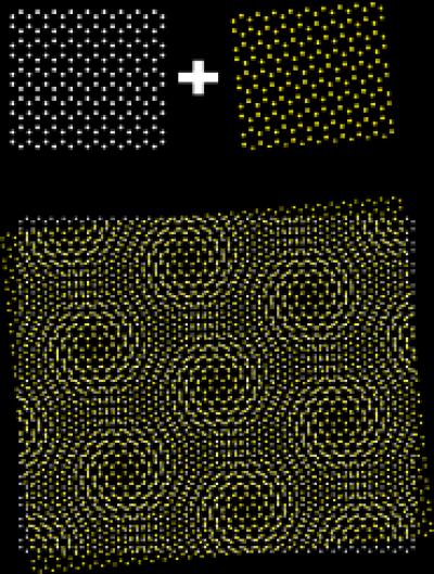
When a sheet of graphene sits atop a sheet of boron nitride at an angle, a secondary hexagonal pattern emerges that determines how electrons flow across the sample (credit: Brian LeRoy)
University of Arizona (UA) physicists are making discoveries with graphene that may advance electronic circuit technology.
Resembling chicken wire on a nano scale, graphene — single sheets of graphite — is only one atom thick, making it the world’s thinnest material. Two million graphene sheets stacked up would not be as thick as a credit card.
The tricky part physicists have yet to figure out how to control the flow of electrons through the material, a necessary prerequisite for putting it to work in any type of electronic circuit. Graphene behaves very different than silicon, the material currently used in semiconductors.
Graphene has been proposed for a wide range of electronics applications ranging from transistors to sensors. However, one of the major difficulties is controlling (turning the current on and off) in a graphene device, Brian LeRoy, an assistant professor in the University of Arizona’s department of physics, explained to KurzweilAI.
“Unlike silicon, which has a band gap [a range of energy states], graphene does not have a band gap. So there is always current flowing, even in the ‘off’ state, which wastes energy.”
“If you want to make a transistor for example, you need to be able to stop the flow of electrons,” LeRoy said “But in graphene, the electrons just keep going. It’s difficult to stop them. This strange behavior makes it difficult to control where electrons are going in graphene.”
Boron nitride and the graphene superlattice
However, the UA physicists have found that boron nitride influences how the electrons tunnel through the graphene. The results open up new ways of controlling the electron flow through graphene.
Mounting graphene on boron nitride prevents some of the electrons from tunneling, a first step toward a more controlled electron flow.
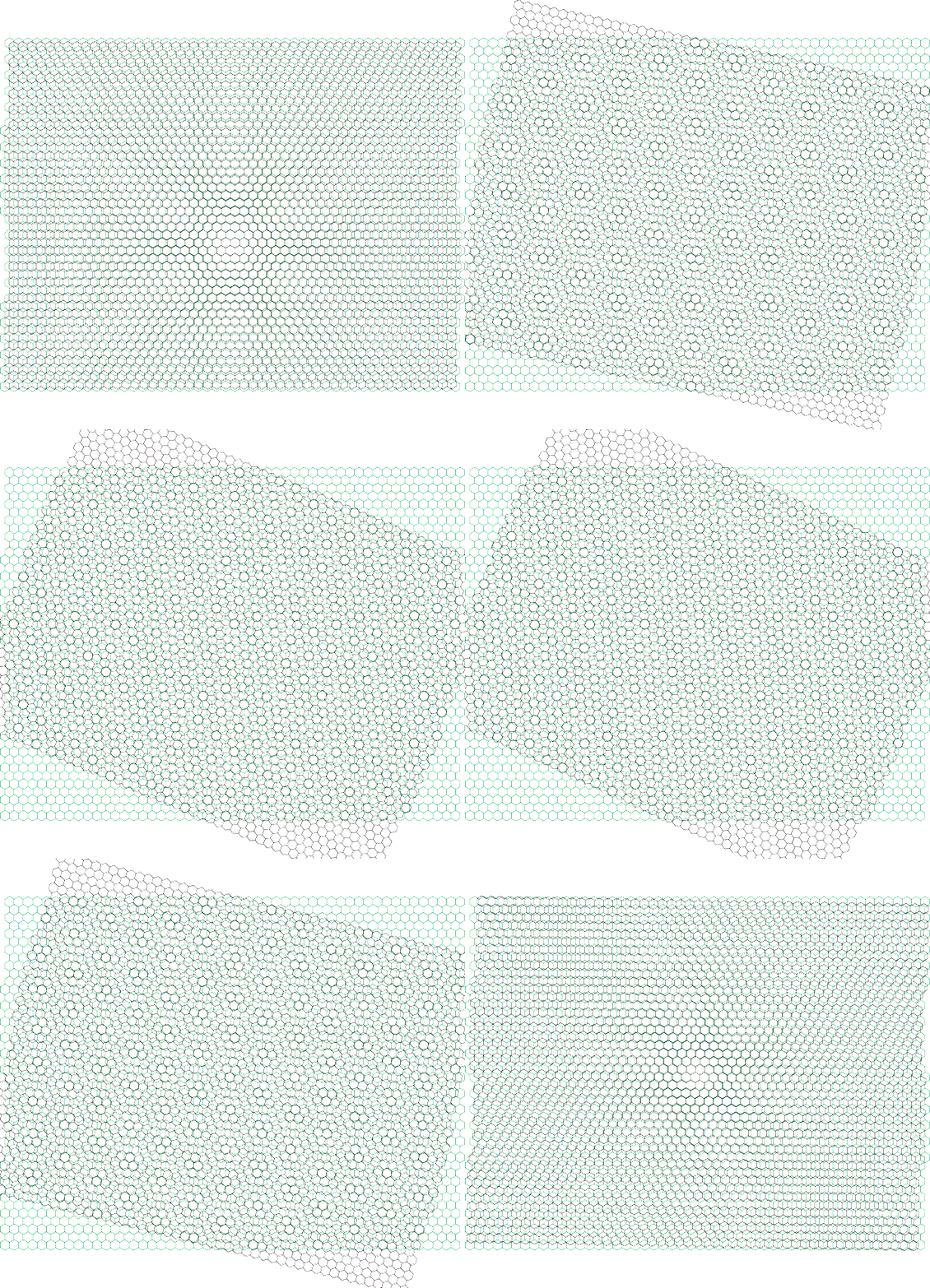
The group achieved this feat by placing graphene sheets onto boron nitride at certain angles, resulting in the hexagonal structures in both materials overlapping in such a way that secondary, larger hexagonal patterns are created — a superlattice.
If the angle is just right, they found, a point is reached where almost no electrons go through.
“You could say we created holes in the wall,” LeRoy said, “and as soon as the wall has holes in it, we find that some of the [electrons] no longer go through. It’s the opposite of what you would expect. That shows you how weird this is. It’s all due to those relativistic quantum effects.”
“The effect depends on the size of the hexagonal pattern resulting from the overlapping sheets,” explained Matthew Yankowitz, a first-year graduate student in LeRoy’s lab and the study’s lead author. “It’s a purely electronic effect brought about by the structure of the two materials and how they sit on top of each other,” Yankowitz said. “It’s similar to the Moiré pattern you see when someone wears a striped shirt on TV.”
“With our scanning tunneling microscope, we can get an image of each superlattice and measure its size,” Yankowitz said. “We take a picture and see what the pattern looks like. If the hexagonal pattern is too small, the samples are no good and we throw them out.”
Where is graphene on the microprocessor roadmap?
The discovery puts the technology a bit closer to someday being able to actually control the flow of electrons through the graphene. If it becomes possible to someday automate this process, graphene-based microelectronics might be well on their way to propel us from the silicon age to the graphene age.
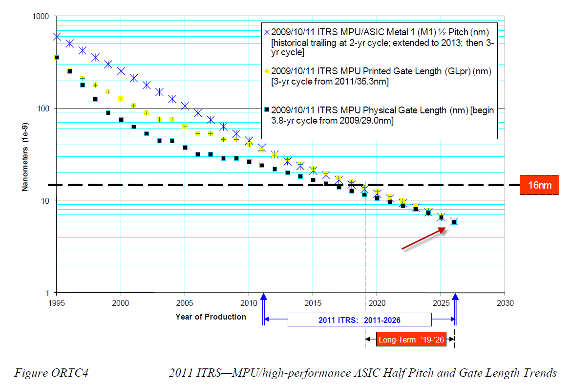
So we asked LeRoy how graphene relates to the ITRS roadmap (see below), which shows how small a microprocessor gate length is forecast to be in what year (currently goes out to 6 nm in 2026). “I would say that graphene exceeds the roadmap in most ways. It is already as thin as possible (a single atomic layer). (We’ve asked for further details. Check back later today. — Ed.)
“There is no reason that it can not be scaled down to very small gate sizes because it remains conductive even at the size of a single benzene ring. The speed of graphene transistors has already been shown to exceed 100 GHz, which is partly due to the high mobility of the electrons in graphene.”
Ref.: Matthew Yankowitz, et al., Emergence of superlattice Dirac points in graphene on hexagonal boron nitride, Nature Physics, 2012; [DOI:10.1038/nphys2272]

