An artificial synapse for future miniaturized portable ‘brain-on-a-chip’ devices
January 22, 2018

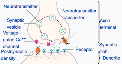
Biological synapse structure (credit: Thomas Splettstoesser/CC)
MIT engineers have designed a new artificial synapse made from silicon germanium that can precisely control the strength of an electric current flowing across it.
In simulations, the researchers found that the chip and its synapses could be used to recognize samples of handwriting with 95 percent accuracy. The engineers say the new design, published today (Jan. 22) in the journal Nature Materials, is a major step toward building portable, low-power neuromorphic chips for use in pattern recognition and other machine-learning tasks.
Controlling the flow of ions: the challenge
Researchers in the emerging field of “neuromorphic computing” have attempted to design computer chips that work like the human brain. The idea is to apply a voltage across layers that would cause ions (electrically charged atoms) to move in a switching medium (synapse-like space) to create conductive filaments in a manner that’s similar to how the “weight” (connection strength) of a synapse changes.
There are more than 100 trillion synapses (in a typical human brain) that mediate neuron signaling in the brain, strengthening some neural connections while pruning (weakening) others — a process that enables the brain to recognize patterns, remember facts, and carry out other learning tasks, all at lightning speeds.
Instead of carrying out computations based on binary, on/off signaling, like current digital chips, the elements of a “brain on a chip” would work in an analog fashion, exchanging a gradient of signals, or “weights” — much like neurons that activate in various ways (depending on the type and number of ions that flow across a synapse).
But it’s been difficult to control the flow of ions in existing synapse designs. These have multiple paths that make it difficult to predict where ions will make it through, according to research team leader Jeehwan Kim, PhD, an assistant professor in the departments of Mechanical Engineering and Materials Science and Engineering, a principal investigator in MIT’s Research Laboratory of Electronics and Microsystems Technology Laboratories.
“Once you apply some voltage to represent some data with your artificial neuron, you have to erase and be able to write it again in the exact same way,” Kim says. “But in an amorphous solid, when you write again, the ions go in different directions because there are lots of defects. This stream is changing, and it’s hard to control. That’s the biggest problem — nonuniformity of the artificial synapse.”
Epitaxial random access memory (epiRAM)

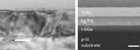
(Left) Cross-sectional transmission electron microscope image of 60 nm silicon-germanium (SiGe) crystal grown on a silicon substrate (diagonal white lines represent candidate dislocations). Scale bar: 25 nm. (Right) Cross-sectional scanning electron microscope image of an epiRAM device with titanium (Ti)–gold (Au) and silver (Ag)–palladium (Pd) layers. Scale bar: 100 nm. (credit: Shinhyun Choi et al./Nature Materials)
So instead of using amorphous materials as an artificial synapse, Kim and his colleagues created an new “epitaxial random access memory” (epiRAM) design.
They started with a wafer of silicon. They then grew a similar pattern of silicon germanium — a material used commonly in transistors — on top of the silicon wafer. Silicon germanium’s lattice is slightly larger than that of silicon, and Kim found that together, the two perfectly mismatched materials could form a funnel-like dislocation, creating a single path through which ions can predictably flow.*
This is the most uniform device we could achieve, which is the key to demonstrating artificial neural networks,” Kim says.
Testing the ability to recognize samples of handwriting
As a test, Kim and his team explored how the epiRAM device would perform if it were to carry out an actual learning task: recognizing samples of handwriting — which researchers consider to be a practical test for neuromorphic chips. Such chips would consist of artificial “neurons” connected to other “neurons” via filament-based artificial “synapses.”

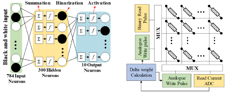
Image-recognition simulation. (Left) A 3-layer multilayer-perception neural network with black and white input signal for each layer in algorithm level. The inner product (summation) of input neuron signal vector and first synapse array vector is transferred after activation and binarization as input vectors of second synapse arrays. (Right) Circuit block diagram of hardware implementation showing a synapse layer composed of epiRAM crossbar arrays and the peripheral circuit. (credit: Shinhyun Choi et al./Nature Materials)
They ran a computer simulation of an artificial neural network consisting of three sheets of neural layers connected via two layers of artificial synapses, based on measurements from their actual neuromorphic chip. They fed into their simulation tens of thousands of samples from the MNIST handwritten recognition dataset**, commonly used by neuromorphic designers.
They found that their neural network device recognized handwritten samples 95.1 percent of the time — close to the 97 percent accuracy of existing software algorithms running on large computers.
A chip to replace a supercomputer
The team is now in the process of fabricating a real working neuromorphic chip that can carry out handwriting-recognition tasks. Looking beyond handwriting, Kim says the team’s artificial synapse design will enable much smaller, portable neural network devices that can perform complex computations that are currently only possible with large supercomputers.
“Ultimately, we want a chip as big as a fingernail to replace one big supercomputer,” Kim says. “This opens a stepping stone to produce real artificial intelligence hardware.”
This research was supported in part by the National Science Foundation. Co-authors included researchers at Arizona State University.
* They applied voltage to each synapse and found that all synapses exhibited about the same current, or flow of ions, with about a 4 percent variation between synapses — a much more uniform performance compared with synapses made from amorphous material. They also tested a single synapse over multiple trials, applying the same voltage over 700 cycles, and found the synapse exhibited the same current, with just 1 percent variation from cycle to cycle.
** The MNIST (Modified National Institute of Standards and Technology database) is a large database of handwritten digits that is commonly used for training various image processing systems and for training and testing in the field of machine learning. It contains 60,000 training images and 10,000 testing images.
Abstract of SiGe epitaxial memory for neuromorphic computing with reproducible high performance based on engineered dislocations
Although several types of architecture combining memory cells and transistors have been used to demonstrate artificial synaptic arrays, they usually present limited scalability and high power consumption. Transistor-free analog switching devices may overcome these limitations, yet the typical switching process they rely on—formation of filaments in an amorphous medium—is not easily controlled and hence hampers the spatial and temporal reproducibility of the performance. Here, we demonstrate analog resistive switching devices that possess desired characteristics for neuromorphic computing networks with minimal performance variations using a single-crystalline SiGe layer epitaxially grown on Si as a switching medium. Such epitaxial random access memories utilize threading dislocations in SiGe to confine metal filaments in a defined, one-dimensional channel. This confinement results in drastically enhanced switching uniformity and long retention/high endurance with a high analog on/off ratio. Simulations using the MNIST handwritten recognition data set prove that epitaxial random access memories can operate with an online learning accuracy of 95.1%.