Are you ready for atom-thin, ‘invisible’ displays everywhere?
April 4, 2018

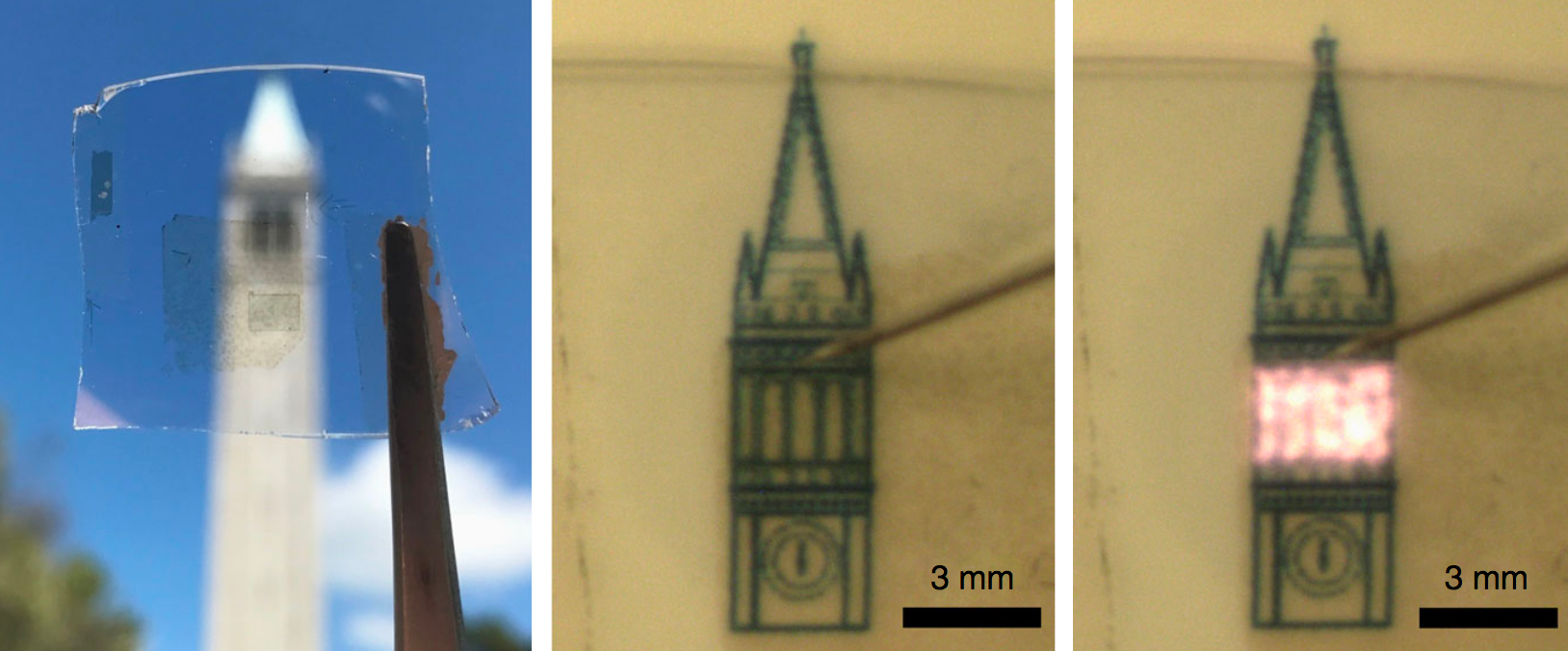
Photograph of a proof-of-concept transparent display (left), and closeups showing the display in off and on states (credit: UC Berkeley)
Bloomberg reported this morning (April 4) that Apple is planning a new iPhone with touchless gesture control and displays that curve inward gradually from top to bottom. Apple’s probable use of microLED technology promises to offer “power savings and a reduced screen thickness when put beside current-generation display panels,”according to Apple Insider.
But UC Berkeley engineers have an even more radical concept for future electronics: invisible displays, using a new atomically thin display technology.
Imagine seeing the person you’re talking to projected onto a blank wall by just pointing at it, or seeing a map pop up on your car window (ideally, matched to the road you’re on) at night and disappear when you wave it off.

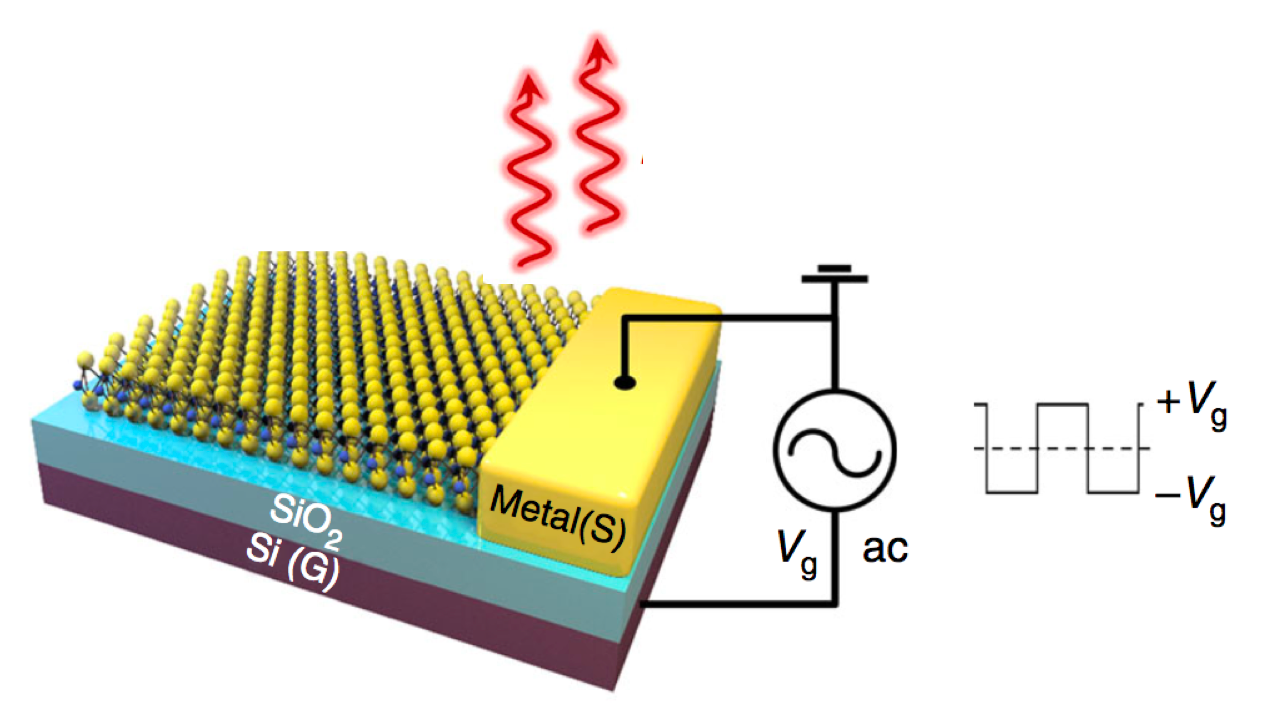
Schematic of transient-electroluminescent device. An AC voltage is applied between the gate (bottom) and source (top) electrodes. Light emission occurs near the source contact edge during the moment when the AC signal switches its polarity from positive to negative (and vice versa), so both positive and negative charges are present at the same time in the semiconductor, creating light. (credit: Der-Hsien Lien et al./Nature Communications)
The secret: an ultrathin monolayer semiconductor just three atoms thick — a bright “transient electroluminescent” device that is fully transparent when turned off and that can conform to curved surfaces, even human skin.* The four different monolayer materials each emit different colors of light.
The display is currently a proof-of-concept design — just a few millimeters wide, and about 1 percent efficient (commercial LEDs have efficiencies of around 25 to 30 percent). “A lot of work remains to be done and a number of challenges need to be overcome to further advance the technology for practical applications,” explained Ali Javey, Ph.D., professor of Electrical Engineering and Computer Sciences at Berkeley.
The research study was published March 26 in an open-access paper in Nature Communications. It was funded by the National Science Foundation and the Department of Energy.
* Typically, two contact points are used in a semiconductor-based light emitting device: one for injecting negatively charged particles and one injecting positively charged particles. Making contacts that can efficiently inject these charges is a fundamental challenge for LEDs, and it is particularly challenging for monolayer semiconductors since there is so little material to work with. The Berkeley research team engineered a way around this: designing a new device that only requires one contact on the transition-metal dichalcogenide (MoS2, WS2, MoSe2, and WSe2) monolayer instead of two contacts.
Abstract of Large-area and bright pulsed electroluminescence in monolayer semiconductors
Transition-metal dichalcogenide monolayers have naturally terminated surfaces and can exhibit a near-unity photoluminescence quantum yield in the presence of suitable defect passivation. To date, steady-state monolayer light-emitting devices suffer from Schottky contacts or require complex heterostructures. We demonstrate a transient-mode electroluminescent device based on transition-metal dichalcogenide monolayers (MoS2, WS2, MoSe2, and WSe2) to overcome these problems. Electroluminescence from this dopant-free two-terminal device is obtained by applying an AC voltage between the gate and the semiconductor. Notably, the electroluminescence intensity is weakly dependent on the Schottky barrier height or polarity of the contact. We fabricate a monolayer seven-segment display and achieve the first transparent and bright millimeter-scale light-emitting monolayer semiconductor device.