Biodegradable electronics that vanish in the body
September 28, 2012

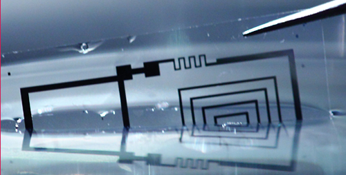
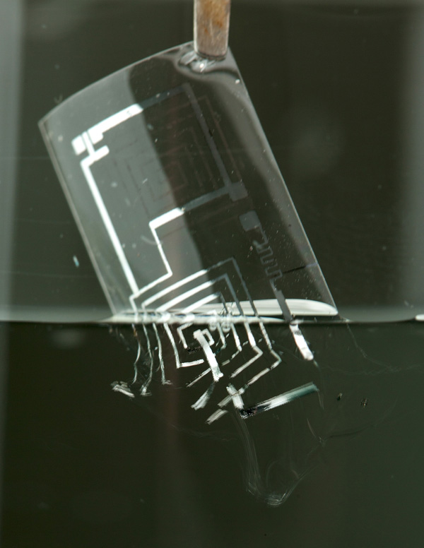
A biodegradable integrated circuit during dissolution in water (credit: Beckman Institute, University of Illinois and Tufts University)
A new type of biodegradable electronics technology that could revolutionize medical implants, environmental monitors, and consumer devices has been developed by researchers at the University of Illinois, in collaboration with Tufts University and Northwestern University.
“We refer to this type of technology as transient electronics,” said John A. Rogers, the Lee J. Flory-Founder Professor of Engineering at the U. of I., who led the multidisciplinary research team.
Three application areas for this biodegradable technology appear particularly promising:
- Medical implants that perform important diagnostic or therapeutic functions for a useful amount of time and then simply dissolve and resorb in the body, such as intravascular stents, porous bodies for drug delivery, and sutures.
- Environmental monitors, such as wireless sensors that are dispersed after a chemical spill, that degrade over time to eliminate any ecological impact.
- Consumer electronic systems or sub-components that are compostable, to reduce electronic waste streams generated by devices that are frequently upgraded, such as cellphones or other portable devices.
Transient electronic systems
Transient electronic systems harness and extend various techniques that the Rogers’ group has developed over the years for making tiny, yet high-performance electronic systems out of ultrathin sheets of silicon.
In transient applications, the sheets are so thin that they completely dissolve in a few days when immersed in biofluids. Together with soluble conductors and dielectrics, based on magnesium and magnesium oxide, these materials provide a complete palette for a wide range of electronic components, sensors, wireless transmission systems and more.
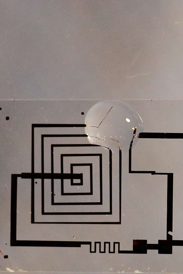
The team has built transient transistors, diodes, wireless power coils, temperature and strain sensors, photodetectors, solar cells, radio oscillators and antennas, and even simple digital cameras. All of the materials are biocompatible and, because they are extraordinarily thin, they can dissolve in even minute volumes of water.
The researchers encapsulate the devices in silk. The structure of the silk determines its rate of dissolution — from minutes to days, weeks or, potentially, years.
“The different applications that we are considering require different operating time frames,” Rogers said. “A medical implant that is designed to deal with potential infections from surgical site incisions is only needed for a couple of weeks.
But for a consumer electronic device, you’d want it to stick around at least for a year or two. The ability to use materials science to engineer those time frames becomes a critical aspect in design.”
Since the group uses silicon, the industry standard material for integrated circuits, they can make highly sophisticated devices in ways that exploit well-established designs by introducing just a few additional tricks in layout, manufacturing and supporting materials.
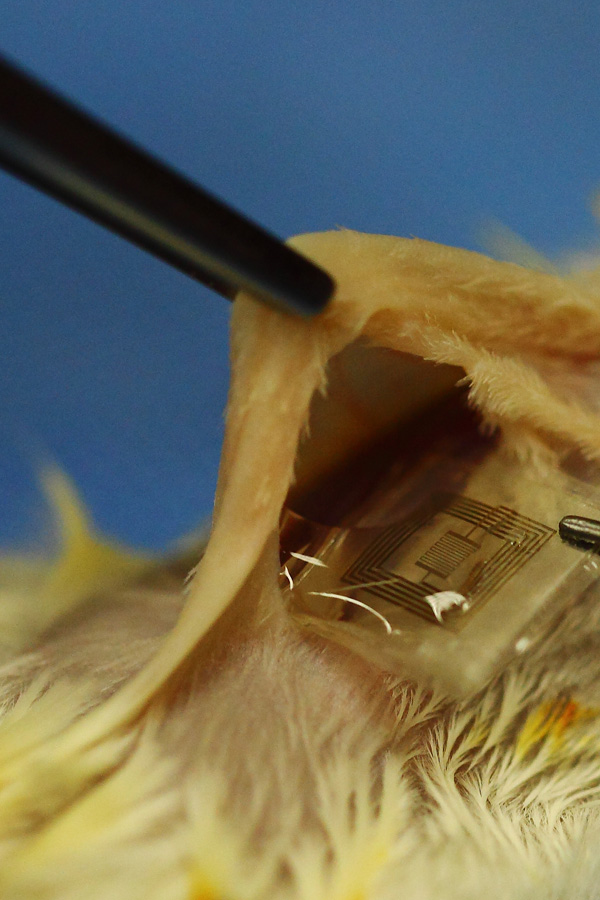
The researchers have already demonstrated several system-level devices, including a fully transient 64-pixel digital camera and an implantable applique designed to monitor and prevent bacterial infection at surgical incisions, successfully demonstrated in rats.
Next, the researchers are further refining these and other devices for specific applications, conducting more animal tests, and working with a semiconductor foundry to explore high-volume manufacturing possibilities.
“It’s a new concept, so there are lots of opportunities, many of which we probably have not even identified yet” Rogers said. “We’re very excited. These findings open up entirely new areas of application, and associated directions for research in electronics.”
The Defense Advanced Research Projects Agency supported this work.
How it works
The transient electronic devices demonstrated by the researchers use magnesium electrodes and interconnects, magnesium oxide gate and interlayer dielectrics, with very thin sheets of silicon, called nanomembranes, as the semiconductor.
Silicon dissolves in biofluids, but at rates that are so slow that conventional silicon wafers would take hundreds of years to degrade. By contrast, nanomembranes are thin enough to dissolve in a few days or weeks, depending on their thickness, in only a few droplets of water. Yet they are thick enough to enable high-quality semiconductor devices, such as transistors, diodes and others.
Both silicon and magnesium occur naturally in the environment and have been explored for various medical implants and drug-delivery systems, although in bulk structural forms. The amount of each material in a transient electronic system is much smaller than the recommended daily allowance — the magnesium is even less than that found in a multivitamin — or even less than normal physiological levels. At the same time, it is enough for sophisticated electronics with integrated functions.
The devices are encapsulated in layers of silk, collected from silkworm cocoons, dissolved and recrystallized. By carefully controlling the crystal structure of the silk, the researchers can control the dissolution rate, so that they can tune the lifespan of a transient device for a specific application. The timescales for dissolution can range from a few minutes to days, weeks, months or potentially, years, all depending on the silk packaging.


