Black phosphorus improves optical communication for chip interconnects
March 3, 2015

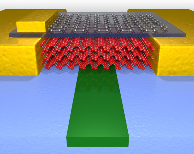
This illustration shows a high-performance photodetector, which uses few-layer black phosphorus (red) to sense light in the waveguide (green). Graphene (gray) is also used to tune the performance. (credit: University of Minnesota College of Science and Engineering)
University of Minnesota researchers have found that an ultrathin black phosphorus film — only 20 layers of atoms — allows for high-speed data communication on nanoscale optical circuits. Black phosphorus is a crystaline form of the element phosphorus.
The devices showed vast improvement in efficiency over comparable devices using graphene.
The work by University of Minnesota Department of Electrical and Computer Engineering Professors Mo Li and Steven Koester and graduate students Nathan Youngblood and Che Chen was published Monday March 2 in Nature Photonics.
Chip-makers are attempting to cram more processor cores on a single chip, but getting all those processors to communicate with each other has been a key challenge for researchers. So the goal is to find materials that will allow high-speed, on-chip communication using light.
Due to its unique properties, black phosphorus can be used to detect light very effectively, making it desirable for optical applications. The University of Minnesota team created intricate optical circuits in silicon and then laid thin flakes of black phosphorus over these structures.
Rivals germanium without the limits for optical circuits
The University of Minnesota team demonstrated that the performance of the black phosphorus photodetectors even rivals that of comparable devices made of germanium — considered the gold standard in on-chip photodetection. Germanium, however, is difficult to grow on silicon optical circuits, while black phosphorus and other two-dimensional materials can be grown separately and transferred onto any material, making them much more versatile.
The team also showed that the devices could be used for real-world applications by sending high-speed optical data over fibers and recovering it using the black phosphorus photodetectors. The group demonstrated data speeds up to 3 gigabits per second.
“Even though we have already demonstrated high speed operation with our devices, we expect higher transfer rates through further optimization,” said Nathan Youngblood, the lead author of the study. “Since we are the first to demonstrate a high speed photodetector using black phosphorus, more work still needs to be done to determine the theoretical limits for a fully optimized device.”
Semiconductor properties
While black phosphorus has much in common with graphene — another two-dimensional material — the materials have significant differences, the most important of which is the existence of an energy gap, often referred to as a “band gap.”
Materials with a band gap, known as semiconductors, are a special group of materials that only conduct electricity when the electrons in that material absorb enough energy for them to “jump” the band gap. This energy can be provided through heat, light, and other means.
While graphene has proven useful for a wide variety of applications, its main limitation is its lack of a band gap. This means that graphene always conducts a significant amount of electricity, and this “leakage” makes graphene devices inefficient. In essence, the device is “on” and leaking electricity all the time.
Black phosphorus, on the other hand, has a widely-tunable band gap that varies depending on how many layers are stacked together. This means that black phosphorus can be tuned to absorb light in the visible range but also in the infrared. This large degree of tunability makes black phosphorus a unique material that can be used for a wide range of applications—from chemical sensing to optical communication.
Additionally, black phosphorus is a “direct-band” semiconductor, meaning it has the potential to efficiently convert electrical signals back into light. Combined with its high performance photodetection abilities, black phosphorus could also be used to generate light in an optical circuit, making it a one-stop solution for on-chip optical communication, with no restriction to a specific substrate or wavelength.
The University of Minnesota research was funded by the Air Force Office of Scientific Research and the National Science Foundation.
Abstract of Waveguide-integrated black phosphorus photodetector with high responsivity and low dark current
Layered two-dimensional materials have demonstrated novel optoelectronic properties and are well suited for integration in planar photonic circuits. Graphene, for example, has been utilized for wideband photodetection. However, because graphene lacks a bandgap, graphene photodetectors suffer from very high dark current. In contrast, layered black phosphorous, the latest addition to the family of two-dimensional materials, is ideal for photodetector applications due to its narrow but finite bandgap. Here, we demonstrate a gated multilayer black phosphorus photodetector integrated on a silicon photonic waveguide operating in the near-infrared telecom band. In a significant advantage over graphene devices, black phosphorus photodetectors can operate under bias with very low dark current and attain an intrinsic responsivity up to 135 mA W−1 and 657 mA W−1 in 11.5-nm- and 100-nm-thick devices, respectively, at room temperature. The photocurrent is dominated by the photovoltaic effect with a high response bandwidth exceeding 3 GHz.