Combining materials to make nanoscale 2D electronic components
June 21, 2013

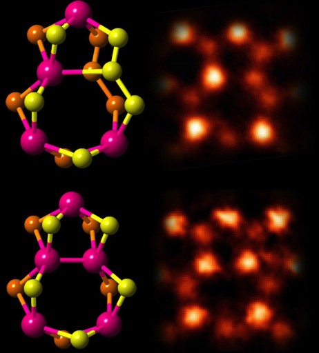
Molybdenum disulfide molecules (molybdenum atoms are cyan and sulfur atoms are orange and yellow) (credit: Oak Ridge National Laboratory)
Scientists at Rice University and Oak Ridge National Laboratory (ORNL) have advanced on the goal of achieving two-dimensional electronics with a method to control the growth of uniform atomic layers of molybdenum disulfide (MDS).
MDS, a semiconductor, is one of three materials needed to make functioning 2D electronic components. The hope is that MDS could be joined with graphene, which has no band gap, and hexagonal boron nitride (hBN), an insulator, to form field-effect transistors, integrated logic circuits, photodetectors and flexible optoelectronics.
The Rice researchers see many possible ways to combine the materials in both two-dimensional and three-dimensional stacks.
“These [three] are very different materials, with different electronic properties and band gaps. Putting one on top of the other would give us a new type of material that we call van der Waals solids,” Ajayan said. “We could put them together in whatever stacking order we need, which would be an interesting new approach in materials science.
The Welch Foundation, the National Science Foundation (NSF), the U.S. Army Research Office, the U.S. Office of Naval Research, the Nanoelectronics Research Corporation and the Department of Energy supported the work.