Could black phosphorus be the next silicon?
July 8, 2015

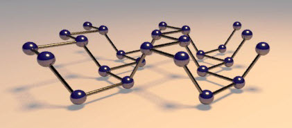
Schematic of the “puckered honeycomb” crystal structure of black phosphorus (credit: Vahid Tayari/McGill University)
An unusual material called “black phosphorus” could emerge as a strong candidate for future energy-efficient transistors, new research from McGill University and Université de Montréal suggests. The material is a form of phosphorus that is similar to graphite (also known as pencil lead and the source of graphene), so it can be exfoliated (separated) easily into single atomic layers known as phosphorene.
Unlike graphene, which acts like a metal, black phosphorus (bP) is a natural semiconductor: it can be switched on and off.
“To lower the operating voltage of transistors, and thereby reduce the heat they generate, we have to get closer and closer to designing the transistor at the atomic level,” says Thomas Szkopek, an associate professor in McGill’s Department of Electrical and Computer Engineering and senior author of an open-access paper published Tuesday (July 7) in Nature Communications.
“Transistors work more efficiently when they are thin, with electrons moving in only two dimensions,” he says. “Nothing gets thinner than a single layer of atoms.”

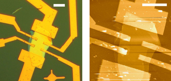
Left: Optical image of an encapsulated black phosphorus FET (field effect transistor). scale bar, 10 μm. (Right) Atomic force microscope image of the same device with encapsulating layer removed. The black phosphorus thickness is 43±2 nm (82±4 atomic layers). Scale bar, 10 μm. (credit: V. Tayari et al./ Nature Communications)
That’s the ideal, but so far, they have only managed to fabricate field effect transistors (FETs) with exfoliated bP layers ranging in thickness from 6nm to 47nm (about 11 to 90 atomic layers). That’s because bP “suffers from photo-oxidation in a reaction that proceeds faster as atomic film thickness is approached,” the authors explain. “The deleterious effects of photo-oxidation are mitigated by using bP layers thicker than a few atomic layers, by encapsulating the bP in a polymer superstrate, and by minimizing exposure to oxygen, water and visible light.”
“There is a great emerging interest around the world in black phosphorus,” Szkopek says. “We are still a long way from seeing atomic layer transistors in a commercial product, but we have now moved one step closer.”
Black arsenic phosphorous
Meanwhile, researchers at USC Viterbi School of Engineering, in collaboration with Technische Universität München, Germany, Universität Regensburg, Germany, and Yale University, have developed a new version of a related 2D material — black arsenic phosphorous (b-AsP) — using a new low-pressure fabrication method that demands less energy, is cheaper, and creates materials have some new electronic and optical properties not available with other 2D materials.
For example, the new b-AsP material can sense long wavelength infrared (LWIR), which is important for LIDAR (light radar) systems used in autonomous (and other new) vehicles, for infrared thermal imaging technology, flexible night vision glasses, and environmental sensing. The paper appeared in Advanced Materials on June 25, 2015.
Abstract of Two-dimensional magnetotransport in a black phosphorus naked quantum well
Black phosphorus (bP) is the second known elemental allotrope with a layered crystal structure that can be mechanically exfoliated to atomic layer thickness. Unlike metallic graphite and semi-metallic graphene, bP is a semiconductor in both bulk and few-layer form. Here we fabricate bP-naked quantum wells in a back-gated field effect transistor geometry with bP thicknesses ranging from 6±1 nm to 47±1 nm. Using a polymer encapsulant, we suppress bP oxidation and observe field effect mobilities up to 900 cm2 V−1 s−1 and on/off current ratios exceeding 105. Shubnikov-de Haas oscillations observed in magnetic fields up to 35 T reveal a 2D hole gas with Schrödinger fermion character in a surface accumulation layer. Our work demonstrates that 2D electronic structure and 2D atomic structure are independent. 2D carrier confinement can be achieved without approaching atomic layer thickness, advantageous for materials that become increasingly reactive in the few-layer limit such as bP.
Abstract of Black Arsenic–Phosphorus: Layered Anisotropic Infrared Semiconductors with Highly Tunable Compositions and Properties
New layered anisotropic infrared semiconductors, black arsenic–phosphorus (b-AsP), with highly tunable chemical compositions and electronic and optical properties are introduced. Transport and infrared absorption studies demonstrate the semiconducting nature of b-AsP with tunable band gaps, ranging from 0.3 to 0.15 eV. These band gaps fall into long-wavelength infrared regime and cannot be readily reached by other layered materials.