Desktop-printing electronic circuits, other nanofabricated devices
July 23, 2013

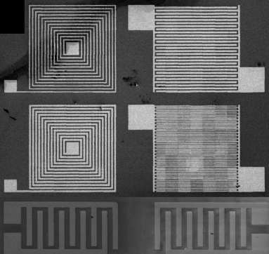
Inductors, capacitors, and a surface acoustic wave transducer created by actuated beam-pen lithography.
A much-anticipated, low-cost, high-resolution desktop nanofabrication tool promises to revolutionize fabrication of electronic circuits and other nanofabricated devices, according to a new study by Northwestern University researchers.
“With this breakthrough, we can construct very high-quality materials and devices, such as processing semiconductors over large areas, said Chad A. Mirkin, senior author of the study and a world-renowned pioneer in the field of nanoscience.
And we can do it with an instrument slightly larger than a printer and in a matter of hours, he added.
Currently, most nanofabrication is done in multibillion-dollar centralized facilities called foundries — analogous to printing documents in centralized printing shops before desktop publishing.
Now, instead of requiring millions of dollars in instrumentation costs, the new tool is poised to prototype a diverse range of functional structures, from making electronic circuits to gene chips and protein arrays, and building patterns that control how stem cells differentiate.
How nanofabrication with beam-pen lithography works

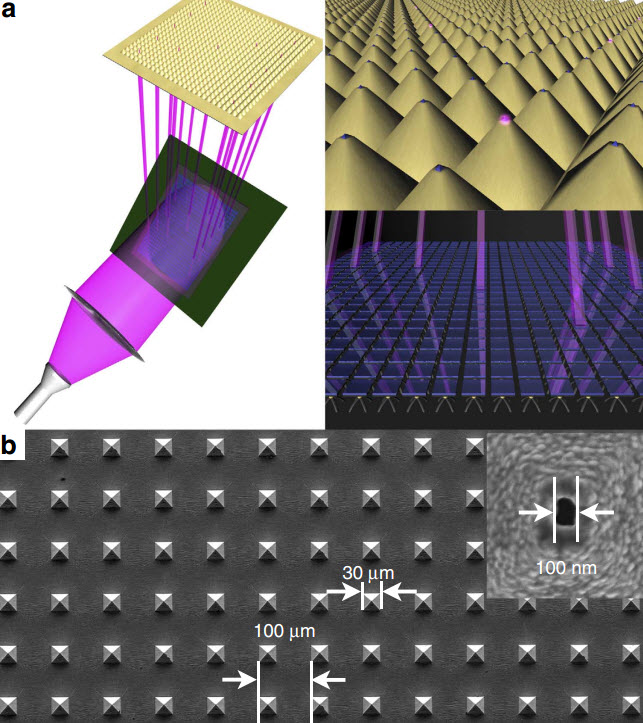
Schematic of actuated BPL. (a) Schematic of the principle
of operation of actuated BPL. A digital micromirror device (DMD) is illuminated with ultraviolet light, which is selectively directed onto the back of a near-field aperture array. (b) Scanning electron microscope (SEM) image of section of the BPL tip array. Each pyramidal pen in the array has a sub-wavelength aperture that has been opened in a parallel fashion. Mirkin’s team’s advances in desktop nanofabrication are based on beam-pen lithography (BPL) pen arrays, structures that consist of an array of polymeric pyramids, each coated with an opaque layer with a 100 nanometer aperture at the tip.
Using a digital micromirror device (similar to a projector), a single beam of light is broken up into thousands of individual beams, each channeled down the back of different pyramidal pens within the array and through the apertures at the tip of each pen.
This nanofabrication tool allows one to rapidly process substrates coated with photosensitive materials (“resists”) and generate structures that span the macro-, micro- and nanoscales, all in one experiment.
Key advances made by Mirkin’s team include developing the hardware, writing the software to coordinate the direction of light onto the pen array, and constructing a system to make all of the pieces of this instrument work together in synchrony.
This approach allows each pen to write a unique pattern and for these patterns to be stitched together into functional devices.
“There is no need to create a mask or master plate every time you want to create a new structure,” Mirkin said.
“You just assign the beams of light to go in different places and tell the pens what pattern you want generated.”
Commercialization in two years
Because the materials used to make the desktop nanofabrication tool are easily accessible, commercialization may be as little as two years away, Mirkin said.

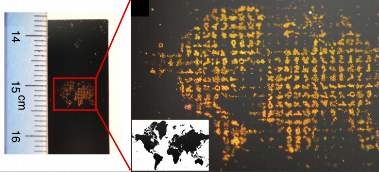
Left: photographic image of a map of the world) ninety nine square mm in size. Right: magnified photograph of the pattern, with an inset depicting the image from which the mosaic was generated.
In the meantime, his team is working on building more devices and prototypes.
In the paper, Mirkin explains how his lab produced a map of the world at nanoscale resolution, a feat never before achieved with a scanning probe instrument.
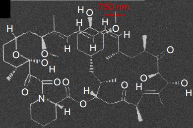
Not only that, but closer inspection with a microscope reveals that this image is actually a mosaic of individual chemical formulae made up of nanoscale points.
Making this pattern showcases the instrument’s capability of simultaneously writing centimeter-scale patterns with nanoscale resolution.

SEM image showing a molecule in the map’s “land” region
Mirkin is the George B. Rathmann Professor of Chemistry in the Weinberg College of Arts and Sciences and a professor of medicine, chemical and biological engineering, biomedical engineering and materials science and engineering. He also is the director of Northwestern’s International Institute for Nanotechnology.
This study was supported by a DARPA/MTO Award, an AOARD Award, AFOSR Awards, NSF Awards, DoD/NPS/NSSEF Fellowship Awards, the Chicago Biomedical Consortium with support from Searle Funds at The Chicago Community Trust, and a CCNE initiative of NIH Award.
(Credit for all images: X. Liao et al./Northwestern University)