How phase change materials could combine RAM’s speed + flash’s non-volatility and capacity
June 22, 2012

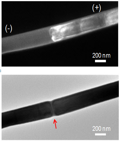
Top: Dark field transmission electron microscopy image of an electrically programmed phase change nanowire. White contrast shows the jammed dislocation cloud along the cross-section. Bottom: Bright field image of the nanowire after amorphization. The red arrow shows the amorphous mark spanning the nanowire cross-section. (Credit: University of Pennsylvania)
University of Pennsylvania researchers have found out how memory devices switch between phases (o’s and1’s), which could help engineers make memory storage devices faster, non-volatile, and high-capacity.
Background
“For many years there has been a push to find memory storage that is at once scalable, non-volatile, and fast,” Agarwal said. “Phase change materials could meet all of those criteria, but the problem is that we don’t know much about how these materials actually work.”
Some kinds of memory, like a computer’s RAM, can switch between states very quickly, allowing for the computation necessary to run programs. But this kind of memory is “volatile” in that it needs a constant supply of power to maintain its states.
Other kinds of memory, like the kind found on a flash drive, is non-volatile in that it retains its data even after the power is turned off. This kind of memory, however, has low switching speeds. Researchers have long attempted to find a “universal memory” which combines both non-volatility and high switching speeds, along with scalability, the ability to store large amounts of data.
Phase change materials, or PCMs, are ideal candidates for universal memory. PCM storage devices are now starting to become commercially available, but their efficiency is hindered by the fact that the actual mechanics of their phase change are not well understood.
The phases these PCMs switch between are different arrangements of their internal atomic structure. They begin in a crystalline phase, where their atoms are in an ordered lattice but can switch to a disordered, amorphous phase. The two phases provide much different levels of resistance to electrical current, which is why they are useful for memory storage.
“When you have atoms arranged in a periodic lattice, electrons can flow very easily as they essentially know what to expect,” Agarwal said. “But in the amorphous phase, there is no long-range order; there’s no way to predict the position of atoms going from one part of the material to the other. This scatters the electrons, leading to very high resistance.”
It has been generally believed that the only way to switch between these two states involved heating, which allows the atoms to move out of their lattice positions as the material briefly melts, and rapid cooling, or “quenching,” which solidifies the material into the amorphous phase without giving its atoms the chance to re-crystallize.
“Now we have shown that there is a way to achieve this transition without melting the material,” said Ritesh Agarwal, associate professor in the Department of Materials Science and Engineering in University of Pennsylvania’s School of Engineering and Applied Science, who conducted the research, along with members of his research group.. “We show that short electrical pulses of a few hundred nanosecond duration gradually induce disorder in the material until it amorphizes.”
Their advance was made possible by fashioning a PCM into thin nanowires, rather than a more bulky counterpart. This enabled the researchers to observe the phase change as it happened using a high-resolution transmission electron microscope at an atomic level of detail. Earlier researchers could only look at cross sections of their bulkier PCMs after the switching process was over.
“The pulses create ‘dislocations,’ which are planes of atoms removed from the crystal pattern, disrupting the order locally on an atomic length scale,” said Pavan Nukala, a co-author and member of the Agarwal group. “As we apply more and more pulses, the number of these dislocations start to increase.”
“Eventually, the dislocations start to move down the nanowire in the direction of the current,” Agarwal said. “At a certain point, the number and density of dislocations becomes so huge that they jam in one spot,” causing the material to amorphize the wire at the location of the jam.
“Having the surface amorphize doesn’t give us high resistance ratios because current can still travel through the crystalline interior,” Agarwal said. “Cutting across the entire nanowire completely blocks the current, making for a much better memory devices.
“With surface melting, you can increase the resistance a few times at most, but our observation that the resistance increased by two or three orders of magnitude is another evidence of the new mechanism.”
The PCM that researchers used in their study contained long tellurium-telluriumbonds that can easily slide apart, facilitating the planar dislocations that cause the material to amorphize.
The material, along with a better understanding of the mechanics of its phase change, will provide a starting point for picking the right qualities for future PCMs.
The research was supported by Penn’s Nano/Bio Interface Center, the National Science Foundation, the Office of Naval Research and MIT’s Materials Structures and Devices Center.