How to convert graphene into a semiconductor for scalable production
June 21, 2016

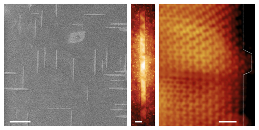
Progressively magnified images (left to right; scale bars: 400, 10, and 1 nm) of graphene nanoribbons grown on germanium semiconductor wafers. (credit: Michael Arnold/University of Wisconsin-Madison)
Graphene can be transformed in the lab from a semimetal into a semiconductor if it is confined into nanoribbons narrower than 10 nm (with controlled orientation and edges), but scaling it up for commercial use has not been possible. Until now.
University of Wisconsin-Madison scientists have discovered how to synthesize narrow, long “one-dimensional” (1-D) nanoribbons (sub-10 nanometers wide) directly on a conventional germanium semiconductor wafer.
That narrow width is not possible with the optical and electron-beam lithography techniques conventionally used in making chips, and integrating graphene nanoribbons onto insulating or semiconducting wafers has also been difficult.
The breakthrough was extremely slow growth (under 5 nanometers per hour), using a new variation of a technique called chemical vapor deposition (CVD), allowing nanoribbons with length-to-width aspect ratios greater than 70 to grow on the surface of a germanium wafer (and with the required smooth “armchair” edges — see the image on the right above).
In addition, this new fabrication process is compatible with existing semiconductor fabrication infrastructure. Appears promising. Let’s see which chipmakers go for it.
The research is described in an open-access article just published in Nature Communications.
Abstract of Direct oriented growth of armchair graphene nanoribbons on germanium
Graphene can be transformed from a semimetal into a semiconductor if it is confined into nanoribbons narrower than 10 nm with controlled crystallographic orientation and well-defined armchair edges. However, the scalable synthesis of nanoribbons with this precision directly on insulating or semiconducting substrates has not been possible. Here we demonstrate the synthesis of graphene nanoribbons on Ge(001) via chemical vapour deposition. The nanoribbons are self-aligning 3° from the Ge 110
110 directions, are self-defining with predominantly smooth armchair edges, and have tunable width to <10 nm and aspect ratio to >70. In order to realize highly anisotropic ribbons, it is critical to operate in a regime in which the growth rate in the width direction is especially slow, <5 nm h−1. This directional and anisotropic growth enables nanoribbon fabrication directly on conventional semiconductor wafer platforms and, therefore, promises to allow the integration of nanoribbons into future hybrid integrated circuits.