IBM announces first 7nm node test chips
July 13, 2015
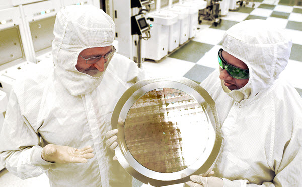
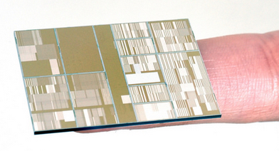
IBM Research has announced the semiconductor industry’s first 7nm (nanometer) node test chips, which could allow for chips with more than 20 billion transistors, IBM believes — a big step forward from today’s most advanced chips, made using 14nm technology.
IBM achieved the 7 nm node through a combination of new materials, tools and techniques, explained Mukesh Khare, VP, IBM Semiconductor Technology Research in a blog post. “In materials, we’re using silicon germanium for the first time in the channels on the chips that conduct electricity. We have employed a new type of lithography in the chip-making process, Extreme Ultraviolet, or EUV, which delivers order-of-magnitude improvements over today’s mainstream optical lithography.”
However, as future technology starts to hit the quantum wall, “there’s no clear path to extend the life of the silicon semiconductor further into the future,” he noted. “The next major wave of progress, the 5 nm node, will be even more challenging than the 7 nm node has been.”
Meanwhile, industry experts consider 7nm technology crucial to meeting the anticipated demands of future cloud computing and Big Data systems, cognitive computing, mobile products and other emerging technologies, says IBM. Part of IBM’s $3 billion, five-year investment in chip R&D (announced in 2014), this accomplishment was the result of a public-private partnership with New York State and joint development alliance with GLOBALFOUNDRIES, Samsung, and equipment suppliers.
When will it be available in products? IBM “declined to speculate on when it might begin commercial manufacturing of this technology generation,” The New York Times reports. Intel’s public roadmap indicates that it’s also working on a 7 nanometer chip, Wired notes.


