Intel invests in keeping Moore’s law alive
July 17, 2012

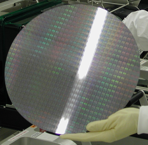
Intel 300mm wafer (credit: Intel)
Intel has invested €2.5 billion ($3.1 billion) in ASML, a Dutch company that dominates the market for the lithographic equipment that etches circuits onto silicon, reports The Economist.
The investment will provide €829m for ASML’s research-and-development efforts and will buy the resulting tools, due in a few years.
Of Intel’s R&D money, €553m will go on technology to make chips on silicon wafers 450mm in diameter. Twice as many chips could be cut from these as from today’s biggest, which are 300mm across.
“The rest of the cash is for extreme ultraviolet (EUV) technology, which the industry hopes will push the width of circuits below today’s frontier of 20 nanometres (billionths of a meter). This will enable more circuitry to be packed onto smaller chips — and allow the life of Moore’s law, which says that the number of transistors on a chip doubles every 18 months or so, to be extended yet again.”