‘Invisible wires’ could improve solar-cell efficiency
November 30, 2015

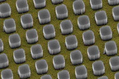
Silicon pillars emerge from nanosize holes in a thin gold film. The pillars funnel 97 percent of incoming light to a silicon substrate, a technology that could significantly boost the performance of conventional solar cells. (credit: Vijay Narasimhan, Stanford University)
Stanford scientists have discovered how to make the electrical wiring on top of solar cells nearly invisible to incoming light, using nanosize silicon pillars to hide the wires. The new design could dramatically boost solar-cell efficiency, the researchers suggest.
A solar cell is basically a semiconductor that converts sunlight into electricity, sandwiched between metal contacts that carry the electrical current generated by the cell. But with current designs, the shiny metal wires on top of the cell reflect sunlight away from the semiconductor surface, reducing the cell’s efficiency.
Now Stanford scientists have discovered how to hide the reflective upper contacts, funneling light directly to the semiconductor below by using silicon pillars to redirect the sunlight before it hits the metallic surface.
Stanford University | “Invisible wires” could boost solar-cell efficiency
Besides gold, the nanopillar architecture will also work with contacts made of silver, platinum, nickel and other metals. In addition to silicon, this new technology can be used with other semiconducting materials for a variety of applications, including photosensors, light-emitting diodes and displays and transparent batteries, as well as solar cells.
The new method aims to improve on a wide variety of methods that have been reported by KurzweilAI.
The findings are published in the journal ACS Nano.
Abstract of Hybrid Metal–Semiconductor Nanostructure for Ultrahigh Optical Absorption and Low Electrical Resistance at Optoelectronic Interfaces
Engineered optoelectronic surfaces must control both the flow of light and the flow of electrons at an interface; however, nanostructures for photon and electron management have typically been studied and optimized separately. In this work, we unify these concepts in a new hybrid metal–semiconductor surface that offers both strong light absorption and high electrical conductivity. We use metal-assisted chemical etching to nanostructure the surface of a silicon wafer, creating an array of silicon nanopillars protruding through holes in a gold film. When coated with a silicon nitride anti-reflection layer, we observe broad-band absorption of up to 97% in this structure, which is remarkable considering that metal covers 60% of the top surface. We use optical simulations to show that Mie-like resonances in the nanopillars funnel light around the metal layer and into the substrate, rendering the metal nearly transparent to the incoming light. Our results show that, across a wide parameter space, hybrid metal–semiconductor surfaces with absorption above 90% and sheet resistance below 20 Ω/□ are realizable, suggesting a new paradigm wherein transparent electrodes and photon management textures are designed and fabricated together to create high-performance optoelectronic interfaces.