Looking inside nanomaterials in 3 dimensions
May 17, 2011

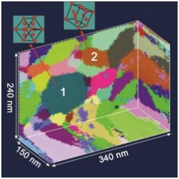
3D map of crystals that have an identical lattice structure but are orientated in different ways, as illustrated by the labels 1 and 2 (credit: H. H. Liu, et al.)
3D mapping of the crystal structure inside a material down to nanometer resolution can be achieved by using a standard transmission electron microscope using a new technique, scientists from Risø DTU (Denmark) and colleagues have found.
The new technique has a resolution 100 times better than existing non-destructive 3D techniques and allows for more precise analysis of the structural parameters in nanomaterials.
Samples must be thinner than a few hundred nanometers. However, this limitation is not a problem for investigations of crystal structures inside nanomaterials, where the average crystal size is less than 100 nanometers.
An important advantage of such 3D methods is that they allow the changes taking place inside a material to be observed directly, the researchers said.
Ref: H. H. Liu, et al., Three-Dimensional Orientation Mapping in the Transmission Electron, Science, 332, 833 (2011)