Manipulating silicon atoms to create future ultra-fast, ultra-low-power chip technology
February 17, 2017

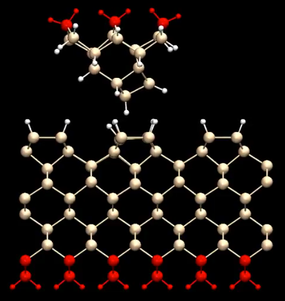
Model showing interactions between atomic-force microscope tip (top) and silicon surface (hydrogen: white; silicon: tan and red), using a new technique for coating the tip with hydrogen — part of a study to create future electronic circuits at the atomic level. (credit: Wolkow Lab)
Imagine a hybrid silicon-molecular computer that uses one thousand times less energy or a cell phone battery that lasts weeks at a time.
University of Alberta scientists, headed by University of Alberta physics professor Robert Wolkow, have taken a major step in that direction by visualizing and geometrically patterning silicon at the atomic level — using an innovative atomic-force microscopy* (AFM) technique. The goal: chip technology that performs dramatically better than today’s CMOS architecture.

(Left) Ball-and-stick theoretical model of the pentacene molecule. (Right) AFM image of pentacene molecule showing the pattern of the bonds in the model. The five hexagonal carbon rings are resolved clearly and even the carbon-hydrogen bonds (white in the model) are imaged. Scale bar: 5 angstroms (0.5 nanometer) (credit: IBM Zurich)
Visualizing bonds in atoms at atomic resolution was first achieved by IBM Zurich scientists in 2009, when they imaged the pentacene molecule on copper. But imaging silicon is a problem: the sharp tip damages the fragile silicon molecules, the researchers note in an open-access paper published in the February 13, 2017 issue of Nature Communications.
To avoid damaging the silicon surface, the researchers created the first hydrogen-covered AFM tip, making it possible to manipulate silicon atoms. It was “a bit like Goldilocks,” PhD student and co-author Taleana Huff explained to KurzweilAI. “There is a sweet-spot region where you are probing the surface without interacting with it. Getting close enough to the surface with just the right parameters allows you to see these bonds materialize.

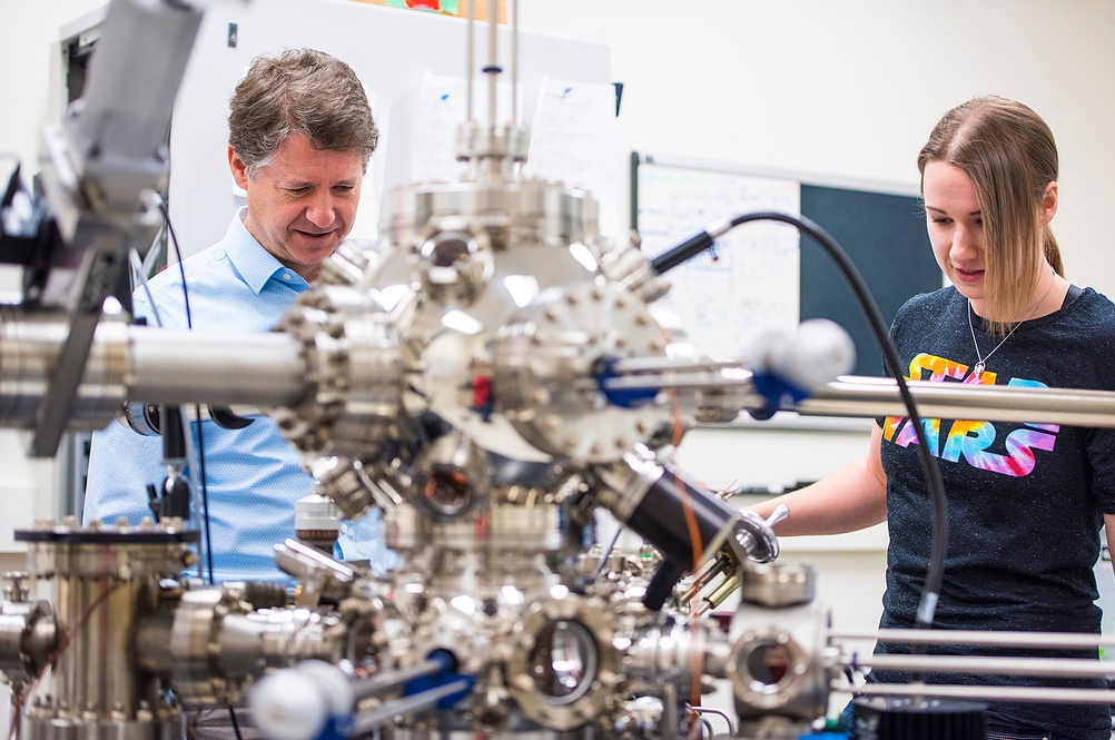
Bob Wolkow and Taleana Huff patterning and imaging electronic circuits at the atomic level (credit: Wolkow Lab)
“If you get too close though, you end up transferring atoms to the surface or, conversely, to the tip, ruining the experiment. A lot of tech and knowledge goes into getting all these settings just right, including a powerful new computational approach that analyzes and verifies the identity of the atoms and bonds.”
Hydrogen-terminated silicon for ultra-fast, ultra-low-power technology
“We see hydrogen-terminated silicon as the platform for a whole new paradigm of efficient and fast silicon-based electronics,” Huff said. “Now that we understand the surface intimately and have these powerful tools and the experience, the next step is to start using the AFM to look at computational elements made using quantum dots [nanoscale semiconductor particles], which we create by removing hydrogen atoms from the silicon surface. When we cleverly pattern them geometrically, these atomic silicon quantum dots can be used to make very fast and incredibly low-power computational patterns.”
The long-term goal is making ultra-fast and ultra-low-power silicon-based circuits that potentially consume one thousand times less power than what is currently on the market, according to the researchers, along with novel quantum applications.
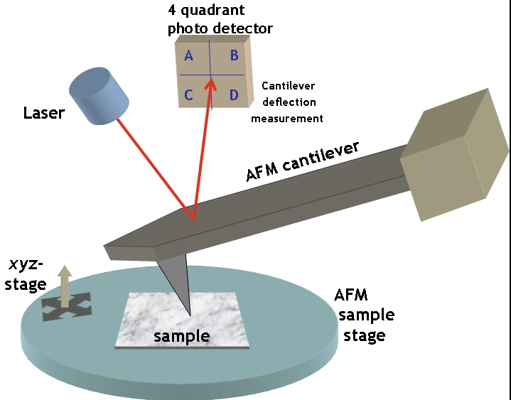
* Typical atomic force microscope (AFM) setup

To image a surface, an AFM sharp tip scans across the sample to detect irregularities in the surface, which cause deflection of the tip and the connected cantilever and generating a topological map of the sample surface. The deflection is measured by reflecting a laser beam off the backside of the cantilever. (credit: CC/Opensource Handbook of Nanoscience and Nanotechnology)
Wolkow Lab | An animation illustrating patterning and imagining electronic circuits at the atomic level. It shows the tip and surface atoms’ relaxation during calculations of a part of the image simulation at small tip-surface distance. The bending and rotation of bonds is visible, giving a sense of the interactions and atomic relaxations involved.
UAlbertaScience | Less is more for atomic-scale manufacturing
This animation represents an electrical current being switched on and off. Remarkably, the current is confined to a channel that is just one atom wide. Also, the switch is made of just one atom. When the atom in the center feels an electric field tugging at it, it loses its electron. Once that electron is lost, the many electrons in the body of the silicon (to the left) have a clear passage to flow through. When the electric field is removed, an electron gets trapped in the central atom, switching the current off. This represents the latest work out of Robert Wolkow’s lab at the University of Alberta.
Abstract of Indications of chemical bond contrast in AFM images of a hydrogen-terminated silicon surface
The origin of bond-resolved atomic force microscope images remains controversial. Moreover, most work to date has involved planar, conjugated hydrocarbon molecules on a metal substrate thereby limiting knowledge of the generality of findings made about the imaging mechanism. Here we report the study of a very different sample; a hydrogen-terminated silicon surface. A procedure to obtain a passivated hydrogen-functionalized tip is defined and evolution of atomic force microscopy images at different tip elevations are shown. At relatively large tip-sample distances, the topmost atoms appear as distinct protrusions. However, on decreasing the tip-sample distance, features consistent with the silicon covalent bonds of the surface emerge. Using a density functional tight-binding-based method to simulate atomic force microscopy images, we reproduce the experimental results. The role of the tip flexibility and the nature of bonds and false bond-like features are discussed.