MITRE-Harvard nanocomputer may point the way to future computer miniaturization
February 6, 2014

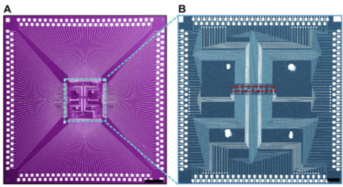
Fabricated nanoelectronic chip. (A) SEM image of the final chip (scale bar, 500 μm). (B) SEM image of the inner layout of the fabricated chip as indicated in the dashed box in A. The red dashed box region corresponds to the chip’s basic three-tile circuit shown. (Scale bar, 100 μm.) (Credit: Jun Yao et al./PNAS)
An interdisciplinary team of scientists and engineers from The MITRE Corporation and Harvard University have taken key steps toward ultra-small electronic computer systems that push beyond the imminent end of Moore’s Law. They designed and assembled, from the bottom up, a functioning, ultra-tiny control computer (nanocontroller) that they say is the densest nanoelectronic system ever built.
The “nanoelectronic finite-state machine” (“nanoFSM”) or nanocomputer measures 0.3 x 0.03 millimeters. It is composed of hundreds of nanowire transistors, each an under-20 nanometers switch. The nanowire transistors use very little power because they are “nonvolatile” — the switches remember whether they are on or off, even when no power is supplied to them.

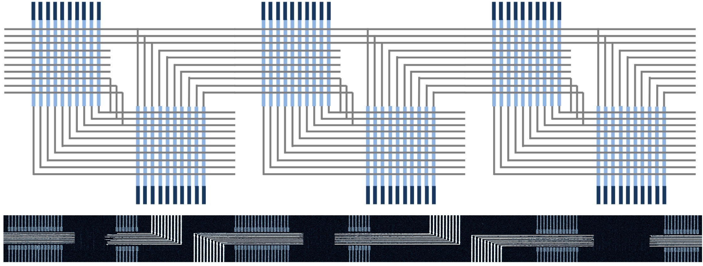
NanoFSM architecture and fabricated system. Depicted are (top) the three “tiles” (modules) in the MITRE architecture for a nanoelectronic finite-state machine (nanoFSM), a fundamental control system. Below it is an SEM micrograph of the functional nanosystem as fabricated by Harvard University according to the FSM architecture. This “3-tile” nanocomputer contains several hundred nanowire transistor switches. (Credit: MITRE)
In the nanoFSM, these nanoswitches are assembled and organized into circuits on several “tiles” (modules). Together, the tiles route small electronic signals around the computer, enabling it to perform calculations and process signals that could be used to control tiny systems, such as miniscule medical therapeutic devices, other tiny sensors and actuators, or even insect-sized robots.
In 2011, the MITRE-Harvard team demonstrated a single such tiny tile capable of performing simple logic operations (see “What ultra-tiny nanocircuits can do“). In their recent collaboration they combined three tiles on a single chip to produce a first-of-its-kind complex programmable nanocomputer.
“It was a challenge to develop a system architecture and nanocircuit designs that would pack the control functions we wanted into such a very tiny system,” according to Shamik Das, chief architect of the nanocomputer, who is also principal engineer and group leader of MITRE’s Nanosystems Group. “Once we had those designs, though, our Harvard collaborators did a brilliant job innovating to be able to realize them.”
Economical bottom-up assembly
Construction of this nanocomputer was made possible by significant advances in processes that assemble with extreme precision dense arrays of the many nanodevices required. These advances also made it possible to manufacture multiple copies of the nanoFSM.
The researchers used a groundbreaking approach in which complex nanosystems can be economically assembled from the bottom up in close conformity to a preexisting design for the first time. Until now, this could be done using the industry’s expensive, top-down lithographic manufacturing methods, but not with bottom-up assembly.
In addition to Das and Ellenbogen, the development team at MITRE included James Klemic, the corporation’s nanotechnology laboratory director. The researchers from MITRE — a pioneer in the nanotechnology field since 1992 — collaborated with a three-person team at Harvard, led by Charles Lieber, a world-leading nanotechnology investigator.
A follow-up article will include an in-depth interview with MITRE researchers. — Editor
Abstract of Proceedings of the National Academy of Sciences paper
Implementation of complex computer circuits assembled from the bottom up and integrated on the nanometer scale has long been a goal of electronics research. It requires a design and fabrication strategy that can address individual nanometer-scale electronic devices, while enabling large-scale assembly of those devices into highly organized, integrated computational circuits. We describe how such a strategy has led to the design, construction, and demonstration of a nanoelectronic finite-state machine. The system was fabricated using a design-oriented approach enabled by a deterministic, bottom–up assembly process that does not require individual nanowire registration. This methodology allowed construction of the nanoelectronic finite-state machine through modular design using a multitile architecture. Each tile/module consists of two interconnected crossbar nanowire arrays, with each cross-point consisting of a programmable nanowire transistor node. The nanoelectronic finite-state machine integrates 180 programmable nanowire transistor nodes in three tiles or six total crossbar arrays, and incorporates both sequential and arithmetic logic, with extensive intertile and intratile communication that exhibits rigorous input/output matching. Our system realizes the complete 2-bit logic flow and clocked control over state registration that are required for a finite-state machine or computer. The programmable multitile circuit was also reprogrammed to a functionally distinct 2-bit full adder with 32-set matched and complete logic output. These steps forward and the ability of our unique design-oriented deterministic methodology to yield more extensive multitile systems suggest that proposed general-purpose nanocomputers can be realized in the near future.