Nanowire measurements could improve computer memory
May 26, 2011

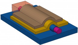
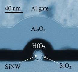
A silicon nanowire is shown surrounded by a stack of thin layers of dielectrics, which store electrical charge (credit: NIST)
The optimal characteristics for nanowire-based charge-trapping memory devices may have been found by physicists at the National Institute of Standards and Technology (NIST).
The technology is based on silicon formed into nanowires, approximately 20 nanometers in diameter. These nanowires form the basis of non-volatile memory.
Nanowire-based devices are being studied extensively as the possible basis for next-generation computer memory because they hold the promise to store information faster and at lower voltage.
Using a combination of software modeling and electrical device characterization, the researchers explored a wide range of structures for dielectrics (thin layers of material that store electrical charge). Based on the understanding they gained, the researchers said an optimal device can be designed.
The design could provide a path to creating portable computers and cell phones that can operate for days between charging sessions, the researchers said.
Ref: X. Zhu, Q. Li, et al., Fabrication, characterization and simulation of high performance Si nanowire-based non-volatile memory cells, Nanotechnology, May 16, 2011, 22 254020 doi: 10.1088/0957-4484/22/25/254020
