New chip architecture may increase qubits in a future quantum computer
May 5, 2015

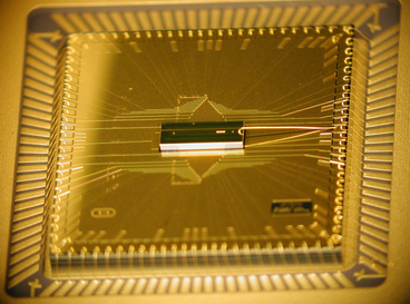
A photograph of the completed BGA trap assembly. The trap chip is at the center, sitting on the larger interposer chip that fans out the wiring. The trap chip surface area is 1mm x 3mm, while the interposer is roughly 1 cm square. (credit: D. Youngner, Honeywell)
Researchers at the Georgia Tech Research Institute and Honeywell International have developed a new ion trap architecture (using ions trapped inside a vacuum chamber and manipulated with lasers) that could increase the density of qubits in future quantum computers.
The GTRI/Honeywell approach uses new microfabrication techniques that allow more electrodes to fit onto the chip. The design borrows ideas from a type of packaging called a ball grid array (BGA), which is used to mount integrated circuits.

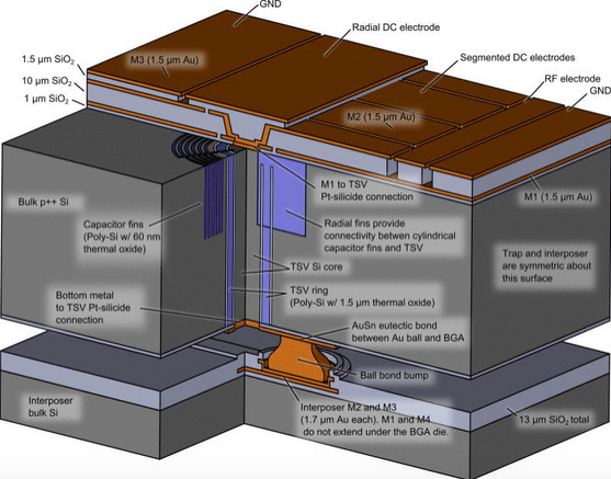
Schematic cross section through BGA trap die and interposer (not to scale) (credit: Nicolas D. Guise et al./Journal of Applied Physics)
The ball grid array design can bring electrical signals directly from the backside of the mount to the surface, thus increasing the potential density of electrical connections.
The researchers also freed up more chip space by replacing area-intensive surface or edge capacitors with trench capacitors and strategically moving wire connections. The space-saving moves allowed tight focusing of an addressing laser beam for fast operations on single qubits.
Miniaturizing
Working with trapped ion qubits currently requires a room full of bulky equipment and several graduate students to make it all run properly, so the researchers say much work remains to be done to shrink the technology.
In the meantime, these advances have applications beyond quantum computing, such as “microfabrication techniques for making miniature atomic devices like sensors, magnetometers and chip-scale atomic clocks,” said GTRI’s Nicholas Guise, who led the research.
The researchers describe the work in an open-access paper appearing today (May 5) in the Journal of Applied Physics.
Abstract of Ball-grid array architecture for microfabricated ion traps
State-of-the-art microfabricated ion traps for quantum information research are approaching nearly one hundred control electrodes. We report here on the development and testing of a new architecture for microfabricated ion traps, built around ball-grid array (BGA) connections, that is suitable for increasingly complex trap designs. In the BGA trap, through-substrate vias bring electrical signals from the back side of the trap die to the surface trap structure on the top side. Gold-ball bump bonds connect the back side of the trap die to an interposer for signal routing from the carrier. Trench capacitors fabricated into the trap die replace area-intensive surface or edge capacitors. Wirebonds in the BGA architecture are moved to the interposer. These last two features allow the trap die to be reduced to only the area required to produce trapping fields. The smaller trap dimensions allow tight focusing of an addressing laser beam for fast single-qubit rotations. Performance of the BGA trap as characterized with 40Ca+ ions is comparable to previous surface-electrode traps in terms of ion heating rate, mode frequency stability, and storage lifetime. We demonstrate two-qubit entanglement operations with 171Yb+ ions in a second BGA trap.