New transistor design enables flexible, high-performance wearable/mobile electronics
October 2, 2017

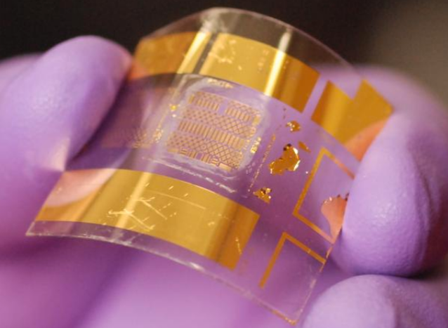
Advanced flexible transistor developed at UW-Madison (photo credit: Jung-Hun Seo/University at Buffalo, State University of New York)
A team of University of Wisconsin–Madison (UW–Madison) engineers has created “the most functional flexible transistor in the world,” along with a fast, simple, inexpensive fabrication process that’s easily scalable to the commercial level.
The development promises to allow manufacturers to add advanced, smart-wireless capabilities to wearable and mobile devices that curve, bend, stretch and move.*
The UW–Madison group’s advance is based on a BiCMOS (bipolar complementary metal oxide semiconductor) thin-film transistor, combining speed, high current, and low power dissipation (heat and wasted energy) on just one surface (a silicon nanomembrane, or “Si NM”).**
BiCMOS transistors are the chip of choice for “mixed-signal” devices (combining analog and digital capabilities), which include many of today’s portable electronic devices such as cellphones. “The [BiCMOS] industry standard is very good,” says Zhenqiang (Jack) Ma, the Lynn H. Matthias Professor and Vilas Distinguished Achievement Professor in electrical and computer engineering at UW–Madison. “Now we can do the same things with our transistor — but it can bend.”
The research was described in the inaugural issue of Nature Publishing Group’s open-access journal Flexible Electronics, published Sept. 27, 2017.***
Making traditional BiCMOS flexible electronics is difficult, in part because the process takes several months and requires a multitude of delicate, high-temperature steps. Even a minor variation in temperature at any point could ruin all of the previous steps.
Ma and his collaborators fabricated their flexible electronics on a single-crystal silicon nanomembrane on a single bendable piece of plastic. The secret to their success is their unique process, which eliminates many steps and slashes both the time and cost of fabricating the transistors.
“In industry, they need to finish these in three months,” he says. “We finished it in a week.”
He says his group’s much simpler, high-temperature process can scale to industry-level production right away.
“The key is that parameters are important,” he says. “One high-temperature step fixes everything — like glue. Now, we have more powerful mixed-signal tools. Basically, the idea is for [the flexible electronics platform] to expand with this.”
* Some companies (such as Samsung) have developed flexible displays, but not other flexible electronic components in their devices, Ma explained to KurzweilAI.
** “Flexible electronics have mainly focused on their form factors such as bendability, lightweight, and large area with low-cost processability…. To date, all the [silicon, or Si]-based thin-film transistors (TFTs) have been realized with CMOS technology because of their simple structure and process. However, as more functions are required in future flexible electronic applications (i.e., advanced bioelectronic systems or flexible wireless power applications), an integration of functional devices in one flexible substrate is needed to handle complex signals and/or various power levels.” — Jung Hun Seo et al./Flexible Electronics. The n-channel, p-channel metal-oxide semiconductor field-effect transistors (N-MOSFETs & P-MOSFETs), and NPN bipolar junction transistors (BJTs) were realized together on a 340-nm thick Si NM layer.
*** Co-authors included researchers at the University at Buffalo, State University of New York, and the University of Texas at Arlington. This work was supported by the Air Force Office Of Scientific Research.
Abstract of High-performance flexible BiCMOS electronics based on single-crystal Si nanomembrane
In this work, we have demonstrated for the first time integrated flexible bipolar-complementary metal-oxide-semiconductor (BiCMOS) thin-film transistors (TFTs) based on a transferable single crystalline Si nanomembrane (Si NM) on a single piece of bendable plastic substrate. The n-channel, p-channel metal-oxide semiconductor field-effect transistors (N-MOSFETs & P-MOSFETs), and NPN bipolar junction transistors (BJTs) were realized together on a 340-nm thick Si NM layer with minimized processing complexity at low cost for advanced flexible electronic applications. The fabrication process was simplified by thoughtfully arranging the sequence of necessary ion implantation steps with carefully selected energies, doses and anneal conditions, and by wisely combining some costly processing steps that are otherwise separately needed for all three types of transistors. All types of TFTs demonstrated excellent DC and radio-frequency (RF) characteristics and exhibited stable transconductance and current gain under bending conditions. Overall, Si NM-based flexible BiCMOS TFTs offer great promises for high-performance and multi-functional future flexible electronics applications and is expected to provide a much larger and more versatile platform to address a broader range of applications. Moreover, the flexible BiCMOS process proposed and demonstrated here is compatible with commercial microfabrication technology, making its adaptation to future commercial use straightforward.