Piezoelectricity in a 2D semiconductor
December 24, 2014

To measure and demonstrate piezoelectrically generated membrane stress, an MoS2 film (yellow) was suspended on two posts and clamped by two gold electrodes. The film was indented by a scanning AFM cantilever probe tip. An electric field was then applied to the film via the two electrodes. It caused piezoelectric-generated mechanical stress, which then changed the load on the cantilever, which was observed by the deflection of a laser beam (credit: Berkeley Lab)
Berkeley Lab scientists have discovered a way to use piezoelectricity — the conversion of mechanical force to electricity and vice versa — with a single layer of molybdenum disulfide (MoS2) semiconductor molecules, which could lead to nanotechnology devices, such as a scanning atomic force microscope (AFM), for extremely small force generation/sensing and other uses.
“Piezoelectricity is a well-known effect in bulk crystals, but this is the first quantitative measurement of the piezoelectric effect in a single layer of molecules that has intrinsic in-plane dipoles,” says Xiang Zhang, director of Berkeley Lab’s Materials Sciences Division.
“The discovery of piezoelectricity at the molecular level not only is fundamentally interesting, but also could lead to tunable piezo-materials and devices for extremely small force generation and sensing,” he added.
Zhang, an international authority on nanoscale engineering, holds the Ernest S. Kuh Endowed Chair at the University of California (UC) Berkeley and is a member of the Kavli Energy NanoSciences Institute at Berkeley. He is the corresponding author of a paper in Nature Nanotechnology describing this research.
Nanoscale piezoelectric materials could provide the lowest possible power consumption for on/off switches in MEMS and other types of electronic computing systems, Zhang explains. However, when material thickness approaches a single molecular layer, the large surface energy can cause piezoelectric structures to be thermodynamically unstable and thus not useful.

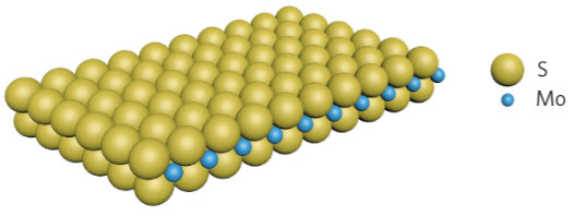
MoS2 atomic structure (credit: Berkeley Lab)
Over the past couple of years, Zhang and his group have been carrying out detailed studies of molybdenum disulfide, a 2D semiconductor that features high electrical conductance comparable to that of graphene, but, unlike graphene, has natural energy band-gaps, which means its conductance can be switched off and on, like a transistor.
Recent calculations predicted the existence of piezoelectricity in these 2D crystals, Zhang said. To test this and determine exactly how much, his team combined (top figure) a laterally applied electric field with nano-indentation in an atomic force microscope to measure piezoelectrically generated membrane mechanical stress.
They recorded a piezoelectric coefficient for molybdenum disulfide of 2.9×10⁻¹⁰ C/m, which is comparable to many widely used materials such as zinc oxide and aluminum nitride and sufficient for use in low-power logic switches and biological sensors that are sensitive to molecular mass limits, the researchers note in the paper.
Piezoelectricity in molybdenum disulfide crystals might also find use in the potential new route to quantum computing and ultrafast data-processing called “valleytronics.” In valleytronics, information is encoded in the spin and momentum of an electron moving through a crystal lattice as a wave with energy peaks and valleys.
This research was supported by Light-Material Interactions in Energy Conversion, an Energy Frontier Research Center led by the California Institute of Technology, in which Berkeley Lab is a major partner. The Energy Frontier Research Center program is supported by DOE’s Office of Science.
Abstract of Observation of piezoelectricity in free-standing monolayer MoS2
Piezoelectricity allows precise and robust conversion between electricity and mechanical force, and arises from the broken inversion symmetry in the atomic structure1, 2, 3. Reducing the dimensionality of bulk materials has been suggested to enhance piezoelectricity4. However, when the thickness of a material approaches a single molecular layer, the large surface energy can cause piezoelectric structures to be thermodynamically unstable5. Transition-metal dichalcogenides can retain their atomic structures down to the single-layer limit without lattice reconstruction, even under ambient conditions6. Recent calculations have predicted the existence of piezoelectricity in these two-dimensional crystals due to their broken inversion symmetry7. Here, we report experimental evidence of piezoelectricity in a free-standing single layer of molybdenum disulphide (MoS2) and a measured piezoelectric coefficient of e11 = 2.9 × 10⁻¹⁰ C m−1. The measurement of the intrinsic piezoelectricity in such free-standing crystals is free from substrate effects such as doping and parasitic charges. We observed a finite and zero piezoelectric response in MoS2 in odd and even number of layers, respectively, in sharp contrast to bulk piezoelectric materials. This oscillation is due to the breaking and recovery of the inversion symmetry of the two-dimensional crystal. Through the angular dependence of electromechanical coupling, we determined the two-dimensional crystal orientation. The piezoelectricity discovered in this single molecular membrane promises new applications in low-power logic switches for computing and ultrasensitive biological sensors scaled down to a single atomic unit cell8, 9.