Printed photonic crystal mirrors shrink on-chip lasers
July 25, 2012
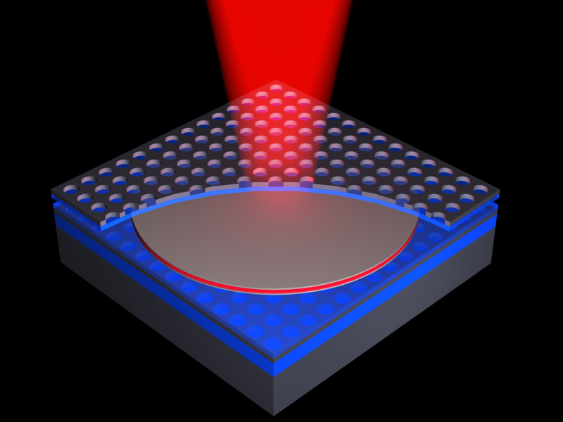
Artist’s representation of the proposed on-chip laser design, created via transfer printing of photonic crystal between layers of silicon nanomembrane (credit: Hongjun Yang)
Electrical engineers at The University of Texas at Arlington and the University of Wisconsin-Madison have devised a new laser for on-chip optical connections that could give computers a huge boost in speed and energy efficiency.
At just 2 microns (millionths of meter) in height, the surface-emitting laser’s vastly lower profile could make it cheaper and easier for manufacturers to integrate high-speed optical data connections into the microprocessors powering the next generation of computers.
Traditionally, edge-emitter lasers are considered as the candidate for on-chip optical links. But since mirrors are hard to form in such lasers and because the lasers occupy a large chip area, researchers have been challenged to find a practical way to monolithically integrate the mirrors on silicon chips.
Surface-emitting lasers necessary for high-speed optical links between computer cores can be 20 to 30 microns tall, compared to a 1.5-microns wavelength optically connected chip
“It sits tall on the chip, like a tower,” says Zhenqiang Ma, a UW-Madison professor of electrical and computer engineering. “That is definitely not acceptable.”
Weidong Zhou, a UT Arlington professor of electrical engineering, says one challenge was integrating light into silicon chips, as silicon itself is not an efficient light emitter.
Photonic crystal mirrors
Zhou and Ma have collaborated to shrink on-chip lasers in recent years with funding from the U.S. Air Force Office of Scientific Research, Army Research Office and Defense Advanced Research Projects Agency.
As a solution, the researchers propose replacing layers and layers of reflectors necessary in the traditional distributed Bragg reflector laser design with two highly reflective photonic crystal mirrors.
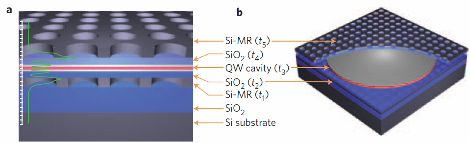
MR-VCSEL on silicon. a, Schematic of a lasing cavity that consists of five layers (t1–t5), with a total thickness of 1–2 wavelengths. An InGaAsP quantum well is sandwiched between two single-layer Si-MRs. Also shown is a simulated electrical field distribution in the cavity for a lasing mode at 1,527 nm, with a confinement factor of 6%. b, A cutout view of the complete MR-VCSEL. (Credit: H. Yang et al./Nature Photonics)
Composed of compound semiconductor quantum-well materials, each mirror is held in place with silicon nanomembranes, using extremely thin layers of a silicon nanomembrane transfer printing process. One layer of photonic crystal is equal to about 15 to 30 layers of dielectric reflectors found in conventional lasers.
In addition to their larger size, reflectors for conventional lasers are made of materials grown only at very high temperatures, which means they can damage the chip they are placed upon during production. Since fabrication via transfer printing can occur at much lower temperatures, Zhou and Ma hope their laser design can be used to place optical links on silicon chips with much less wasted material, time and effort.
Optical data links already exist at the largest scales of data networks — the Internet’s backbone is composed mainly of fiber-optic links between countries, cities and houses. But currently, that data moves over to slower metal connections and wiring as it travels from a regional hub to your house, your computer and eventually between the CPU cores within of the processor powering your machine.
“In the future, you’ll see a move to optical at each step,” Ma says. “The last step is within the chip, module to module optical links on the chip itself.”
Through Semerane Inc., the Texas-based startup Zhou and Ma founded, the two hope to implement their production process in functional on-chip photonic crystal membrane lasers that could eventually be part of the next generation high-speed computer processors, with optical connections all along the chain.
“The co-existence of photonics with electronics on the chip level shall enable multi-functional energy-efficient super-chips for applications in computing, communications, sensing, and imaging,” Zhou says.