Probe captures high-resolution images of nanomaterials
March 30, 2011

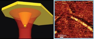
Coaxial probe (left) for imaging a carbon nanotube and chemical map of carbon nanotube (right) with chemical and topographical information at each pixel (credit: Weber et al.)
Scientists at Berkeley Lab’s Molecular Foundry have pioneered a new chemical mapping method that provides unprecedented insight into materials at the nanoscale, says Alexander Weber-Bargioni, a postdoctoral scholar in the Imaging and Manipulation of Nanostructures Facility at the Foundry.
The team designed and fabricated a coaxial antenna capable of focusing light at the nanoscale using a state-of-the-art focused ion beam tool. The antenna consists of gold wrapped around a silicon nitride atomic force microscope (AFM) tip and serves as an optical probe for structures, with 20-nanometer resolution.
The probe provides enough enhancement to report the chemical fingerprint at each pixel while collecting an image (typically 256 x 256 pixels). This data is then used to generate multiple composition-related “maps,” each with a wealth of chemical information at every pixel.
To test out the capability of the new probe, the team examined carbon nanotubes, which are ideal for this type of interactive investigation because their unmatched electronic and structural properties are sensitive to localized chemical changes.
Researchers seeking information about light-harvesting materials or any dynamic system should benefit from this imaging system, says Weber-Bargioni.
Ref.: Alexander Weber-Bargioni, et al., “Hyperspectral nanoscale imaging on dielectric substrates with coaxial optical antenna scan probes,” Nano Letters, January 24, 2011