Sculpting a Nano ‘World’
April 30, 2010 | Source: Technology Review
IBM researchers have invented a low-cost, fast, and relatively simple fabrication tool capable of reliably creating 3-D features as small as 15 nanometers.
The silicon tip is cantilevered like those used in atomic force microscopy (AFM), enabling it to apply nanonewtons of force to the surface. But unlike AFM, the tip is heated, so when it touches the substrate, the thermal energy at the tip is sufficient to break weak bonds within the material.
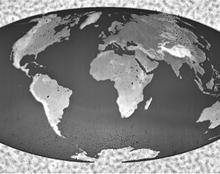
World map with 500,000 pixels and 15-nanometer features drawn in just two minutes (Advanced Materials)