Skyscraper-style carbon-nanotube chip design ‘boosts electronic performance by factor of a thousand’
December 9, 2015
Researchers at Stanford and three other universities are creating a revolutionary new skyscraper-like high-rise architecture for computing based on carbon nanotube materials instead of silicon.
In Rebooting Computing, a special issue (in press) of the IEEE Computer journal, the team describes its new approach as “Nano-Engineered Computing Systems Technology,” or N3XT.
Suburban-style chip layouts create long commutes and regular traffic jams in electronic circuits, wasting time and energy, they note.
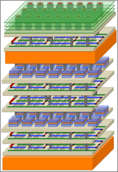
N3XT will break data bottlenecks by integrating processors and memory-like floors in a skyscraper and by connecting these components with millions of “vias,” which play the role of tiny electronic elevators.
The N3XT high-rise approach will move more data, much faster, using far less energy, than would be possible using low-rise circuits, according to the researchers.
Stanford researchers including Associate Professor Subhasish Mitra and Professor H.-S. Philip Wong have “assembled a group of top thinkers and advanced technologies to create a platform that can meet the computing demands of the future,” Mitra says.
“When you combine higher speed with lower energy use, N3XT systems outperform conventional approaches by a factor of a thousand,” Wong claims.
Carbon nanotube transistors
Engineers have previously tried to stack silicon chips but with limited success, the researchers suggest. Fabricating a silicon chip requires temperatures close to 1,800 degrees Fahrenheit, making it extremely challenging to build a silicon chip atop another without damaging the first layer. The current approach to what are called 3-D, or stacked, chips is to construct two silicon chips separately, then stack them and connect them with a few thousand wires.
But conventional 3-D silicon chips are still prone to traffic jams and it takes a lot of energy to push data through what are a relatively few connecting wires.
The N3XT team is taking a radically different approach: building layers of processors and memory directly atop one another, connected by millions of vias that can move more data over shorter distances that traditional wire, using less energy, and immersing computation and memory storage into an electronic super-device.
The key is the use of non-silicon materials that can be fabricated at much lower temperatures than silicon, so that processors can be built on top of memory without the new layer damaging the layer below. As in IBM’s recent chip breakthrough (see “Method to replace silicon with carbon nanotubes developed by IBM Research“), N3XT chips are based on carbon nanotube transistors.
Transistors are fundamental units of a computer processor, the tiny on-off switches that create digital zeroes and ones. CNTs are faster and more energy-efficient than silicon processors, and much thinner. Moreover, in the N3XT architecture, they can be fabricated and placed over and below other layers of memory.
Among the N3XT scholars working at this nexus of computation and memory are Christos Kozyrakis and Eric Pop of Stanford, Jeffrey Bokor and Jan Rabaey of the University of California, Berkeley, Igor Markov of the University of Michigan, and Franz Franchetti and Larry Pileggi of Carnegie Mellon University.
New storage technologies
Team members also envision using data storage technologies that rely on materials other than silicon. This would allow for the new materials to be manufactured on top of CNTs, using low-temperature fabrication processes.
One such data storage technology is called resistive random-access memory, or RRAM (see “‘Memristors’ based on transparent electronics offer technology of the future“). Resistance slows down electrons, creating a zero, while conductivity allows electrons to flow, creating a one. Tiny jolts of electricity switch RRAM memory cells between these two digital states. N3XT team members are also experimenting with a variety of nanoscale magnetic storage materials.
Just as skyscrapers have ventilation systems, N3XT high-rise chip designs incorporate thermal cooling layers. This work, led by Stanford mechanical engineers Kenneth Goodson and Mehdi Asheghi, ensures that the heat rising from the stacked layers of electronics does not degrade overall system performance.
Mitra and Wong have already demonstrated a working prototype of a high-rise chip. At the International Electron Devices Meeting in December 2014 they unveiled a four-layered chip made up of two layers of RRAM memory sandwiched between two layers of CNTs (see “Stanford engineers invent radical ‘high-rise’ 3D chips“).
In their N3XT paper they ran simulations showing how their high-rise approach was a thousand times more efficient in carrying out many important and highly demanding industrial software applications.
