Super-black carbon nanotubes make spacecraft instruments more sensitive
July 23, 2013

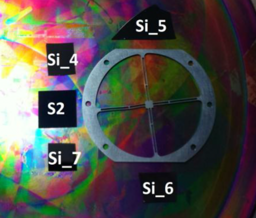
Australia’s Melbourne Centre for Nanofabrication applied a catalyst layer using atomic layer deposition to this occulter mask (credit: NASA)
A team led by John Hagopian, an optics engineer at NASA’s Goddard Space Flight Center in Greenbelt, Md., has demonstrated that it can grow a uniform layer of carbon nanotubes through the use of another emerging technology called atomic layer deposition or ALD.
The super-black nanotechnology that promises to make spacecraft optical instruments more sensitive without enlarging their size.
“The significance of this is that we have new tools that can make NASA instruments more sensitive without making our telescopes bigger and bigger” by suppressing stray light, Hagopian said.
“This is particularly applicable to a new class of less-expensive tiny satellites called Cubesats that NASA is developing to reduce the cost of space missions.”
Super Absorbency
During the research, Hagopian tuned the nano-based super-black material, making it ideal for this application, absorbing on average more than 99 percent of the ultraviolet, visible, infrared and far-infrared light that strikes it — a never-before-achieved milestone that now promises to open new frontiers in scientific discovery.
The material consists of a thin coating of multi-walled carbon nanotubes about 10,000 times thinner than a strand of human hair. The NASA team now grows these forests of vertical carbon tubes on commonly used spacecraft materials, such as titanium, copper and stainless steel.
Tiny gaps between the tubes collect and trap light, while the carbon absorbs the photons, preventing them from reflecting off surfaces. Because only a small fraction of light reflects off the coating, the human eye and sensitive detectors see the material as black.
Before growing this forest of nanotubes on instrument parts, however, materials scientists must first deposit a highly uniform foundation or catalyst layer of iron oxide that supports the nanotube growth. For ALD, technicians do this by placing a component or some other substrate material inside a reactor chamber and sequentially pulsing different types of gases to create an ultra-thin film whose layers are literally no thicker than a single atom.
Once applied, scientists then are ready to actually grow the carbon nanotubes. They place the component in another oven and heat the part to about 1,832 F (750 C). While it heats, the component is bathed in carbon-containing feedstock gas.
“The samples we’ve grown to date are flat in shape,” Hagopian explained. “But given the complex shapes of some instrument components, we wanted to find a way to grow carbon nanotubes on three-dimensional parts, like tubes and baffles. The tough part is laying down a uniform catalyst layer. That’s why we looked to atomic layer deposition instead of other techniques, which only can apply coverage in the same way you would spray something with paint from a fixed angle.”