Ultrathin Alternative to Silicon for Future Electronics
November 23, 2010
Researchers with the U.S. Department of Energy’s Lawrence Berkeley National Laboratory (Berkeley Lab) and the University of California (UC) Berkeley, have successfully integrated ultra-thin layers of the semiconductor indium arsenide onto a silicon substrate to create a nanoscale transistor (down to a thickness of 10 nanometers on silicon substrates).
The material’s superior electron mobility and velocity makes it an outstanding candidate for future high-speed, low-power electronic devices.

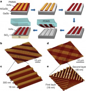
Fabricating an indium oxide (InAs) device starts with a) epitaxially growing and etching InAs into nanoribbon arrays that are get stamped onto a silicon/silica (Si/SiO2 ) substrate; b) and c) InAs nanoribbon arrays on Si/SiO2; d) and e) InAs nanoribbon superstructures on Si/SiO2. (Berkeley Lab)
Adapted from materials provided by Berkeley Lab