Vertical ‘light antennas’ grown from organic semiconductor crystals
October 2, 2015

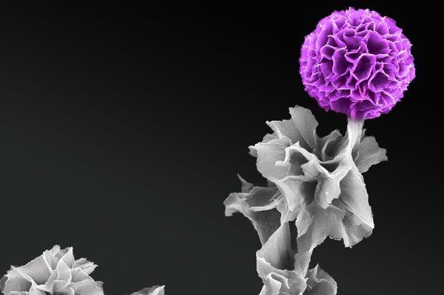
In full bloom: A scanning electron microscopy image of a vertical tetraanaline semiconductor crystal (credit: Jessica Wang)
Materials scientists from the California NanoSystems Institute at UCLA have discovered a way to make organic (carbon-based) semiconductors more powerful and efficient by creating “light antennas.” The thin, pole-like devices could absorb light from all directions, an improvement over today’s wide, flat panels that can only absorb light from one surface.
The breakthrough was in creating an improved structure for one type of organic semiconductor: a building block of a conductive polymer called tetraaniline (TANI). The scientists showed for the first time that tetraaniline crystals could be grown vertically.
The study, led by Richard Kaner, distinguished professor of chemistry and biochemistry and materials science and engineering, was recently published online by the journal ACS Nano.
Growing vertical organic semiconductors

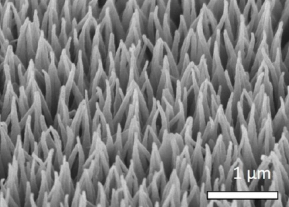
Scanning electron microscope image showing TANI crystals oriented vertically based on graphene (credit: Yue Wang et al./ACS Nano)
The UCLA team grew the tetraaniline crystals vertically from a substrate made of graphene, so the crystals stood up like spikes instead of lying flat as they do when produced using current techniques. Scientists had previously grown crystals vertically in inorganic semiconducting materials, including silicon, but doing it in organic materials has been more difficult.
Tetraaniline is a desirable material for semiconductors because of its particular electrical and chemical properties, which are determined by the orientation of very small crystals it contains. Devices such as solar cells, photosensors, and supercapacitors would work better if the crystals grew vertically because vertical crystals can be packed more densely in the semiconductor, making it more powerful and more efficient at controlling electrical current.
Kaner and his colleagues also developed a one-step method for growing highly ordered, vertically aligned crystals for a variety of organic semiconductors using the same graphene substrate. “This technique enables us to pattern crystals wherever we want,” he said. “You could make electronic devices from these semiconductor crystals and grow them precisely in intricate patterns required for the device you want, such as thin-film transistors or light-emitting diodes.”
The research was supported by the Boeing Company, the National Science Foundation, the U.S. Department of Energy, and the Defense Threat Reduction Agency.
Abstract of Graphene-Assisted Solution Growth of Vertically Oriented Organic Semiconducting Single Crystals
Vertically oriented structures of single crystalline conductors and semiconductors are of great technological importance due to their directional charge carrier transport, high device density, and interesting optical properties. However, creating such architectures for organic electronic materials remains challenging. Here, we report a facile, controllable route for producing oriented vertical arrays of single crystalline conjugated molecules using graphene as the guiding substrate. The arrays exhibit uniform morphological and crystallographic orientations. Using an oligoaniline as an example, we demonstrate this method to be highly versatile in controlling the nucleation densities, crystal sizes, and orientations. Charge carriers are shown to travel most efficiently along the vertical interfacial stacking direction with a conductivity of 12.3 S/cm in individual crystals, the highest reported to date for an aniline oligomer. These crystal arrays can be readily patterned and their current harnessed collectively over large areas, illustrating the promise for both micro- and macroscopic device applications.