A building block for optical quantum networks
February 8, 2013

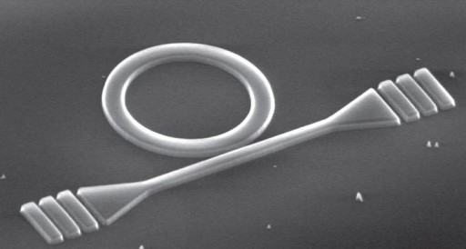
Quantum device with optical resonator (circular object) and waveguide with grating couplers used to couple light into and out of the waveguide.(credit: Andrei Faraon et al./New Journal of Physics)
Another approach to creating optical quantum networks has been developed by Cal Tech, HP, and University of Washington researchers. (See The quantum internet,)
In an optical quantum network, information is carried between points by photons. It could enable quantum computers that are millions of times faster at solving certain problems than what we are used to today.
This new device, which combines a single nitrogen-vacancy center in diamond with an optical resonator and an optical waveguide, could become the memory or the processing element of such a network.
A nitrogen-vacancy center is a defect in the lattice structure of diamond — one of the carbon atoms is replaced by a nitrogen atom and the nearest neighbor carbon atom is missing. The nitrogen-vacancy center has the property of photoluminescence (a substance absorbs photons from a source and then subsequently emits photons).
The emitted photons are special in that they are correlated, or entangled, with the nitrogen-vacancy center that they came from, which is crucial for future experiments that will look to examine this correlation. You cannot get these correlated photons from a normal light source.
The waveguide sends the photons out into a desired direction through gratings at either end.
“One of the holy grails in quantum photonics is to develop networks where optical quantum emitters are interconnected via photons,” said lead author of the study Andrei Faraon.
“In this work we take the first step and demonstrate that photons — the information carriers — from a single nitrogen-vacancy center can be coupled to an optical resonator and then further coupled to a photonic waveguide. We hope that multiple devices of this kind will be interconnected in a photonic network on a chip.”
The study, undertaken by researchers from the California Institute of Technology, Hewlett Packard Laboratories and University of Washington, tested the device by cooling it to temperatures below 10K and shining a green laser onto the nitrogen vacancy to evoke photoluminescence.
The entire device was etched in a diamond membrane that was around 300 nanometers thick.
“The whole idea of these devices is that they are able to be produced en masse. So far, the procedure for mass fabrication is still at the proof-of-concept level, so there is still plenty of work to be done to make it reliable,” continued Professor Faraon.