A low-cost ‘super-resolution’ microscopic optical device
June 22, 2014

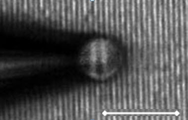
Microsphere-based image of a nanoscale polymer positioned on a silicon substrate. The scale bar is 20 microns. (Credit: Leonid A. Krivitsky et al./Scientific Reports)
A simple, low-cost “super-resolution” optical device using a microsphere capable of imaging surfaces 75 nanometers wide has been developed by researchers at A*STAR Data Storage Institute in Singapore.
Optical-microscope resolution is limited to half the wavelength of light (due to the diffraction limit), so optical microscopes can’t normally resolve structures smaller than a few hundred nanometers.
A*STAR’s Boris Luk’yanchuk and his colleagues previously showed that a micron-scale transparent bead placed on a surface can circumvent the diffraction limit. They demonstrated that light passing through the bead, when collected by a conventional microscope, can create an image of the surface beneath it with a resolution of as low as 50 nanometers.
However, generating a complete two-dimensional map requires scanning the bead across the surface — not easy to perform in a controlled way when the sphere is only 6 microns (millionths of a meter) across. “We have now improved this super-resolution technique by developing a method to controllably move the imaging microspheres,” says team leader Leonid Krivitsky.
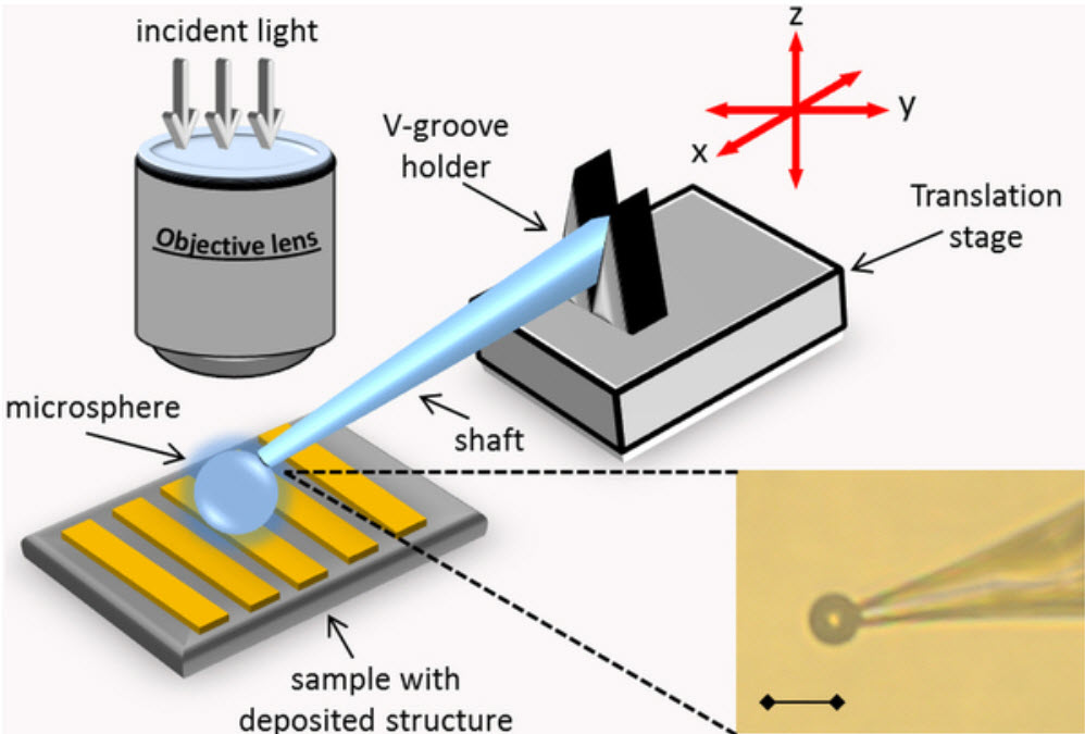
They used a tiny pipette with a tip just 1 or 2 microns wide and fastened it with air suction or UV-curable glue. They then connected the other end of the pipette to a mechanical stage, which could move in steps as small as 20 nanometers, and successfully imaged trial samples with features as small as 75 nanometers.

A microsphere with attached micropipette lies on a sample and is viewed under a microscope. The micropipette (shaft) is attached to a micromanipulator, allowing movement of the microsphere in three dimensions. Inset shows the microscope image of the microsphere. Scale bar: 10 microns. (Credit: Leonid A. Krivitsky et al./Scientific Reports)
Other super-resolution approaches
Other techniques, such as near-field scanning microscopy, can perform sub-diffraction-limit imaging, but commercially available systems range up to around 1 million dollars, they require specific sample preparation, and involve sophisticated image processing algorithms.
KurzweilAI has recently covered two lower-cost super-resolution systems capable or imaging 100 nanometers across. Purdue University’s solution uses three laser beams; the researchers hope to improve it to see objects about 10 nanometers in diameter. Michigan Technological University’s simpler solution uses plasmons on a chip that could be included in cell phones.
“The real advantages of our technique are its simplicity and its price,” says Krivitsky. “The idea could be applied to a variety of superresolution applications such as sample inspection, microfabrication and bioimaging.”
The A*Star super-resolution optical device could conceivably be coupled with either one of two new low-cost optical microscopes also covered on KurzweilAI recently. The University of Washington’s device will turn any smartphone or tablet computer into a handheld microscope that magnifies by 150 times. The standalone Microbescope from 4D Optical is capable of 800x magnification.