Could nanowires be the LEDs of the future?
June 25, 2015

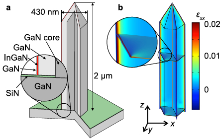
(a) Sketch of an LED nanowire showing the onion-like structure of the layers; (b) Finite element method simulation of strain distribution (credit: Tomas Stankevic, Niels Bohr Institute, University of Copenhagen)
LEDs made from nanowires with an inner core of gallium nitride (GaN) and a outer layer of indium-gallium-nitride (InGaN) — both semiconductors — use less energy and provide better light, according Robert Feidenhans’l, professor and head of the Niels Bohr Institute at the University of Copenhagen.
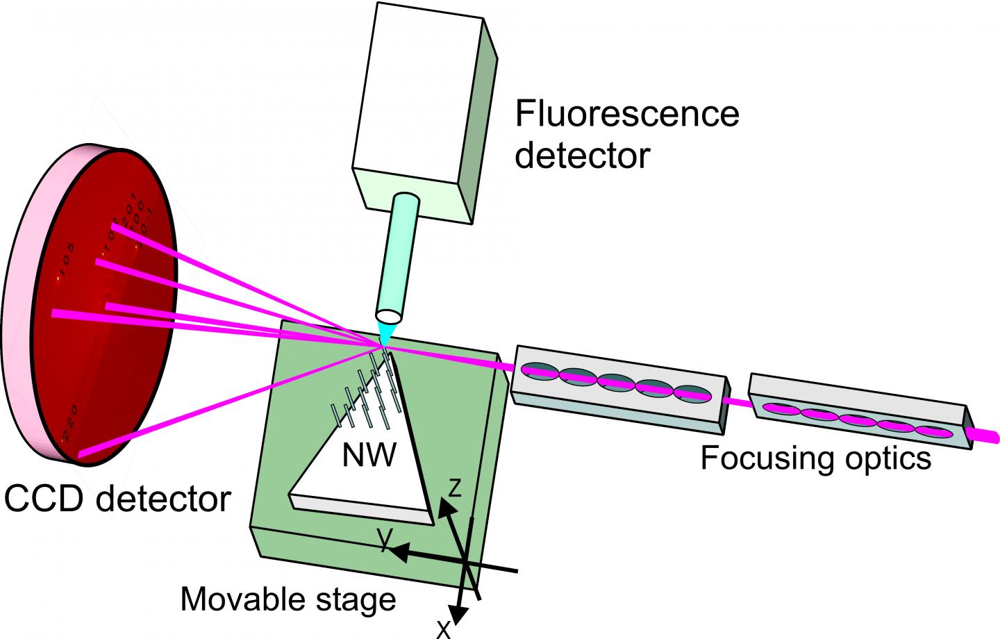
The studies were performed using nanoscale X-ray microscopy in the electron synchrotron at DESY in Hamburg, Germany. The results are published in the journal ACS Nano.
The nanowires could also be used as displays in smart phones, TVs and other forms of lighting within five years, according to the researchers.

A series of nanowires were scanned in a nanofocused X-ray while reflections from the different crystal planes of the nanowires were measured (credit: Tomas Stankevic, Niels Bohr Institute, University of Copenhagen)
Abstract of Fast Strain Mapping of Nanowire Light-Emitting Diodes Using Nanofocused X-ray Beams
X-ray nanobeams are unique nondestructive probes that allow direct measurements of the nanoscale strain distribution and composition inside the micrometer thick layered structures that are found in most electronic device architectures. However, the method is usually extremely time-consuming, and as a result, data sets are often constrained to a few or even single objects. Here we demonstrate that by special design of a nanofocused X-ray beam diffraction experiment we can (in a single 2D scan with no sample rotation) measure the individual strain and composition profiles of many structures in an array of upright standing nanowires. We make use of the observation that in the generic nanowire device configuration, which is found in high-speed transistors, solar cells, and light-emitting diodes, each wire exhibits very small degrees of random tilts and twists toward the substrate. Although the tilt and twist are very small, they give a new contrast mechanism between different wires. In the present case, we image complex nanowires for nanoLED fabrication and compare to theoretical simulations, demonstrating that this fast method is suitable for real nanostructured devices.