Excitons observed in action for the first time
April 23, 2014

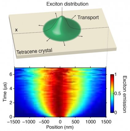
Diagram of an exciton within a tetracene crystal, used in these experiments, shows the line across which data was collected. That data, plotted below as a function of both position (horizontal axis) and time (vertical axis) provides the most detailed information ever obtained on how excitons move through the material.
Scientists at MIT and the City University of New York have imaged excitons’ motions directly for the first time.
A quasiparticle called an exciton — responsible for the transfer of energy within devices such as solar cells, LEDs, and semiconductor circuits — has been understood theoretically for decades. But exciton movement within materials had never been directly observed.
The finding could enable research leading to significant advances in electronics, the researchers say, as well as a better understanding of natural energy-transfer processes, such as photosynthesis.
The research is described in the journal Nature Communications.
According to the researchers, this is the first direct observation of exciton diffusion processes, showing that crystal structure can dramatically affect the diffusion process.
Excitons are at the heart of devices that are relevant to modern technology; the particles determine how energy moves at the nanoscale. The efficiency of devices such as photovoltaics and LEDs depends on how well excitons move within the material.
An exciton, which travels through matter as though it were a particle, pairs an electron, which carries a negative charge, with a place where an electron has been removed, known as a hole. Overall, it has a neutral charge, but it can carry energy. For example, in a solar cell, an incoming photon may strike an electron, kicking it to a higher energy level. That higher energy is propagated through the material as an exciton: The particles themselves don’t move, but the boosted energy gets passed along from one to another.
Knowing how fast exitons move is essential to understanding which aspects of a material’s structure — for example, the degree of molecular order or disorder — might facilitate or slow that motion, the researchers say.
While these experiments were carried out using a material called tetracene — a well-studied archetype of a molecular crystal — the researchers say that the method should be applicable to almost any crystalline or thin-film material. They expect it to be widely adopted by researchers in academia and industry.
Exciton diffusion is also a basic mechanism underlying photosynthesis: plants absorb energy from photons, and this energy is transferred by excitons to areas where it can be stored in chemical form for later use in supporting the plant’s metabolism. The new method might provide an additional tool for studying some aspects of this process, the team says.
The work was supported by the U.S. Department of Energy and by the National Science Foundation, and used facilities of the Eni-MIT Solar Frontiers Center.
Abstract of Nature Communications paper
Transport of nanoscale energy in the form of excitons is at the core of photosynthesis and the operation of a wide range of nanostructured optoelectronic devices such as solar cells, light-emitting diodes and excitonic transistors. Of particular importance is the relationship between exciton transport and nanoscale disorder, the defining characteristic of molecular and nanostructured materials. Here we report a spatial, temporal and spectral visualization of exciton transport in molecular crystals and disordered thin films. Using tetracene as an archetype molecular crystal, the imaging reveals that exciton transport occurs by random walk diffusion, with a transition to subdiffusion as excitons become trapped. By controlling the morphology of the thin film, we show that this transition to subdiffusive transport occurs at earlier times as disorder is increased. Our findings demonstrate that the mechanism of exciton transport depends strongly on the nanoscale morphology, which has wide implications for the design of excitonic materials and devices.