First true 3D microchip created: Cambridge scientists
February 1, 2013

(Credit: stock image)
University of Cambridge scientists have created a new type of microchip that allows information to travel in three dimensions, enabling additional storage capacity on chips.
Currently, microchips can only pass digital information in a very limited way — from either left to right or front to back, the researchers say.
In the future, a 3D microchip would enable additional storage capacity on chips by allowing information to be spread across several layers instead of being compacted into one layer, as is currently the case.
For the research, the Cambridge scientists used a special type of microchip called a spintronic (spin transport electronic) chip, which exploits the electron’s tiny magnetic moment or spin (unlike most of today’s chips, which use charge-based electronic technology). Spintronic chips are increasingly being used in computers, and it is widely believed that within the next few years they will become the standard memory chip.
How to build a 3D chip
To create the microchip, the researchers used an experimental technique called “sputtering.” They effectively made a club sandwich on a silicon chip, consisting of cobalt, platinum, and ruthenium atoms. The cobalt and platinum atoms store the digital information in a similar way to how a hard disk drive stores data. The ruthenium atoms act as messengers, communicating that information between neighboring layers of cobalt and platinum. Each of the layers is only a few atoms thick.
They then used a laser technique called MOKE to probe the data content of the different layers. As they switched a magnetic field on and off they saw in the MOKE signal the data climbing layer by layer from the bottom of the chip to the top. They then confirmed the results using a different measurement method.
“Each step on our spintronic staircase is only a few atoms high,” said Professor Russell Cowburn, lead researcher of the study from the Cavendish Laboratory at the University of Cambridge’s Department of Physics. I find it amazing that by using nanotechnology, not only can we build structures with such precision in the lab, but also using advanced laser instruments, we can actually see the data climbing this nano-staircase step by step.
“This is a great example of the power of advanced materials science. Traditionally, we would use a series of electronic transistors to move data like this. We’ve been able to achieve the same effect just by combining different basic elements such as cobalt, platinum and ruthenium. This is the 21st century way of building things — harnessing the basic power of elements and materials to give built-in functionality.”
First 3D chip?

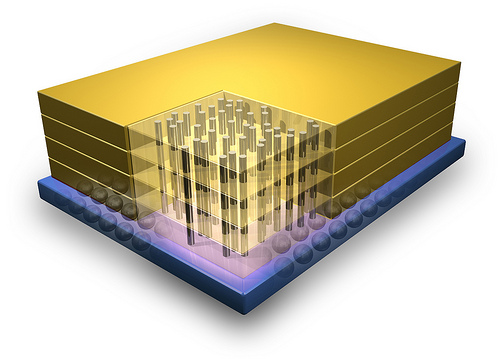
Hybrid memory cube (credit: Micron Technology)
However, in an email, KurzweilAI pointed out to the researchers that at least two 3D chip architectures in fact already exist — Intel’s Tri-Gate transistor and Micron Technology’s Hybrid Memory Cube.
“It depends on what you mean by “3-dimensional,” replied Cowburn. “We mean ‘functionally 3-dimensional,’ i.e., data can move from cell to cell vertically in the same way as it moves cell to cell laterally in today’s devices. That’s why the rest of the press release goes onto to talk about data moving up and down, as opposed to just left to right and back to front.
“The technologies you highlight are ‘structurally 3-dimensional.’ In the case of the Tri-Gate, the gate electrode accesses the channel from more than one side to increase its interaction; but there’s still only 1 functional layer. Memory Cube is slightly closer to what we’re doing, but as far as I can see, data don’t travel vertically from DRAM cell to DRAM cell — they’re just physically stacked on top of each other.”
Cowburn also notes that they were focusing their comments in announcement specifically on spintronic chips. “This is the first time anybody has made a functional 3-dimensional spintronic device; the two technologies you refer to are not spintronic.”
The research was funded by the European Research Council, the Isaac Newton Trust, and the Netherlands Organisation for Scientific Research (NWO).