IBM invents ‘3D nanoprinter’ for microscopic objects
April 25, 2014

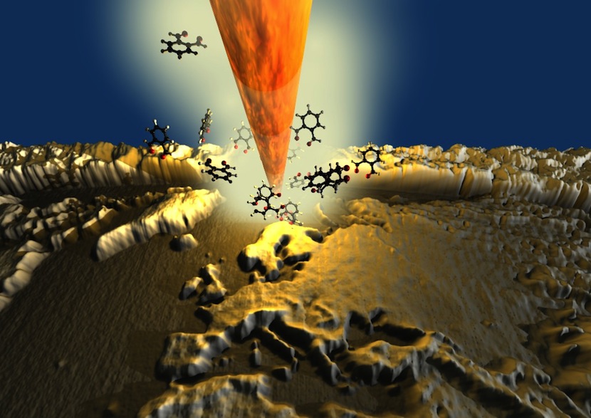
Illustration: a hot tip triggers local decomposition and evaporation of chip substrate material to etch patterns (credit: Advanced Materials)
IBM scientists have invented a tiny “chisel” with a nano-sized heatable silicon tip that creates patterns and structures on a microscopic scale.
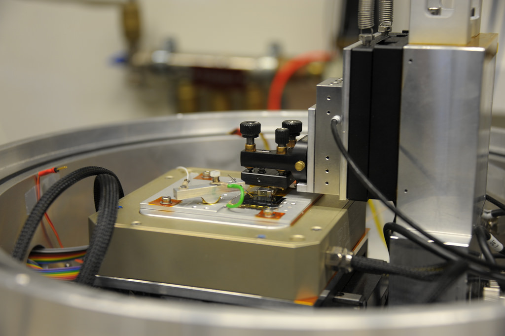
The tip, similar to the kind used in atomic force microscopes, is attached to a bendable cantilever that scans the surface of the substrate material with the accuracy of one nanometer.
Unlike conventional 3D printers, by applying heat and force, the nanosized tip can remove (rather than add) material based on predefined patterns, thus operating like a “nanomilling” machine with ultra-high precision.

IBM scientists have invented a tiny “chisel” with a heatable silicon tip 100,000 times smaller than a sharpened pencil point. Using this nano-sized tip, which creates patterns and structures on a microscopic scale, scientists etched a magazine cover in less than two minutes onto a polymer. The resulting magazine cover is so small at 11 x 14 micrometers that 2,000 can fit on a grain of salt. (Credit: IBM Research)
This new capability could improve the prototyping of new transistor devices, such as tunneling field effect transistors, for more energy efficient and faster electronics for anything from cloud data centers to smartphones.
By the end 2014, IBM hopes to begin exploring the use of this technology for its research with graphene.
“To create more energy-efficient clouds and crunch Big Data faster we need a new generation of technologies including new transistors, but before going into mass production, new techniques are needed for prototyping below 30 nanometers,” said Dr. Armin Knoll, a physicist at IBM Research – Zurich.
“With our new technique, we achieve very high resolution at 10 nanometers at greatly reduced cost and complexity. In particular, by controlling the amount of material evaporated, 3D relief patterns can also be produced at the unprecedented accuracy of merely one nanometer in a vertical direction. Now it’s up to the imagination of scientists and engineers.”
Other applications include nano-sized security tags to prevent the forgery of documents like currency, passports and priceless works of art, and quantum computing and communications (the nano-sized tip could be used to create high quality patterns to control and manipulate light at unprecedented precision).

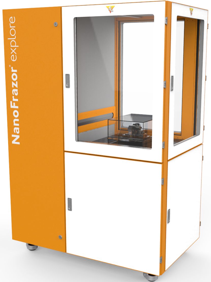
(Credit: Swiss Litho)
The NanoFrazor
IBM has licensed this technology to a startup based in Switzerland called SwissLitho, which is bringing the technology to market under the name NanoFrazor.
Several weeks ago the firm shipped its first NanoFrazor to McGill University’s Nanotools Microfab, where scientists and students will use the tool’s unique fabrication capabilities to experiment with ideas for designing novel nano-devices.
To promote the new technology, scientists etched a microscopic National Geographic Kids magazine cover in 10 minutes onto a polymer. The resulting magazine cover is so small at 11 x 14 micrometers that 2,000 can fit on a grain of salt.
Today (April 25), IBM claimed its ninth GUINNESS WORLD RECORDS title for the Smallest Magazine Cover at the USA Science & Engineering Festival in Washington, D.C. Visible through a Zeiss microscope, the cover will be on display there on April 26 and 27.
Abstract of Science paper
For patterning organic resists, optical and electron beam lithography are the most established methods; however, at resolutions below 30 nanometers, inherent problems result from unwanted exposure of the resist in nearby areas. We present a scanning probe lithography method based on the local desorption of a glassy organic resist by a heatable probe. We demonstrate patterning at a half pitch down to 15 nanometers without proximity corrections and with throughputs approaching those of Gaussian electron beam lithography at similar resolution. These patterns can be transferred to other substrates, and material can be removed in successive steps in order to fabricate complex three-dimensional structures.
Abstract of Advanced Materials paper
3D patterning by means of probe-assisted thermal decomposition has been achieved on phthalaldehyde polymer films with 1 nm vertical resolution and 40 nm lateral resolution. Highly efficient patterning is enabled by a self-amplified depolymerization mechanism. Pixel writing speeds on the order of microseconds are demonstrated.