IBM invests $3 billion to extend Moore’s law with post-silicon-era chips and new architectures
July 10, 2014

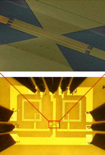
Graphene integrated circuit, the first fabricated from wafer-size graphene, announced by IBM in 2011 (credit: IBM)
IBM announced today it is investing $3 billion for R&D in two research programs to push the limits of chip technology and extend Moore’s law.
The research programs are aimed at “7 nanometer and beyond” silicon technology and developing alternative technologies for post-silicon-era chips using entirely different approaches, IBM says.
IBM will be investing especially in carbon nanoelectronics, silicon photonics, new memory technologies, and architectures that support quantum and cognitive computing.
7 nanometer technology and beyond
IBM researchers and other semiconductor experts predict that semiconductors show promise to scale from today’s 22 nanometers down to 14 and then 10 nanometers in the next several years.
However, scaling down to 7 nanometers by the end of the decade will require significant investment and innovation in semiconductor architectures as well as invention of new tools and techniques for manufacturing, IBM says.
Below 7 nanometers, the challenges dramatically increase, requiring a new kind of materials to power systems of the future, such as carbon nanotubes and graphene; and new computational approaches, such as quantum computing. and neurosynaptic computing.
Carbon Nanotubes. IBM Researchers are exploring whether carbon nanotube (CNT) electronics can replace silicon beyond the 7 nm node. IBM recently demonstrated two-way CMOS NAND gates using 50 nm gate-length carbon nanotube transistors, a first.
IBM also has demonstrated the capability for purifying carbon nanotubes to 99.99%, the highest (verified) purities demonstrated to date, and transistors at 10 nm channel length that show no degradation due to scaling.
Modeling of the electronic circuits suggests that about a five to ten times improvement in performance compared to silicon circuits is possible with CNTs.
Graphene. Graphene — pure carbon in the form of a one-atomic-layer-thick sheet — is an excellent conductor of heat and electricity, and it is also remarkably strong and flexible. Electrons can move in graphene about ten times faster than in commonly used semiconductor materials such as silicon and silicon germanium. That means faster switching transistors. In 2013, IBM demonstrated the world’s first graphene-based integrated-circuit receiver front-end for wireless communications.
IBM’s CMOS Integrated Silicon Nanophotonics chip technology integrates electrical and optical devices on the same piece of silicon, enabling computer chips to communicate using pulses of light (instead of electrical signals). Credit: IBM.
Silicon Photonics. CMOS-integrated silicon photonics integrates functions for optical communications on a silicon chip, and the IBM team has recently designed and fabricated the world’s first monolithic silicon photonics based transceiver with wavelength division multiplexing.
Silicon nanophotonics takes advantage of pulses of light for communication rather than traditional copper wiring and allows large volumes of data to move at rapid speeds between computer chips in servers, large datacenters, and supercomputers, thus alleviating the limitations of congested data traffic and high-cost traditional interconnects.
Silicon nanophotonics technology provides answers to Big Data challenges by seamlessly connecting various parts of large systems and moving terabytes of data via pulses of light through optical fibers.
III-V technologies. III-V (pronounced “three five”) materials have superior efficiency at converting light into power. With more than an order of magnitude higher electron mobility than silicon, integrating III-V materials into CMOS enables higher performance at lower power density, thus allowing for an extension to power/performance scaling to meet the demands of cloud computing and big data systems.

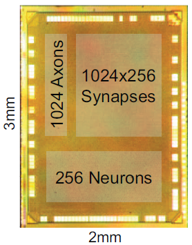
Neurosynaptic core (credit: IBM)
Next-Generation Low-Power Transistors. A potential alternative to today’s power-hungry silicon field-effect transistors are “steep slope” devices. They could operate at much lower voltage and thus dissipate significantly less power.
To reduce the energy consumption in electronics, IBM scientists are researching tunnel field-effect transistors (TFETs), which could achieve a 100-fold power reduction over complementary CMOS transistors.
Quantum Computing. IBM recently demonstrated the first experimental realization of parity check with three superconducting qubits, an essential building block for one type of quantum computer.
Neurosynaptic Computing. This novel technology allows for computing systems that emulate the brain’s computing efficiency, size and power usage.
IBM’s long-term goal is to build a neurosynaptic system with ten billion neurons and 100 trillion synapses, while consuming only one kilowatt of power and occupying less than two liters of volume.