It’s a Small, Small, Small, Small World
April 5, 2001 by Ralph C. Merkle
This introduction to nanotechnology by one of its pioneers is an extended version of the article published in the Feb/Mar 1997 issue of MIT Technology Review. It provides greater technical detail.
Principal Fellow, Zyvex Corporation
Originally published February/March 1997 at www.merkle.com. Published on KurzweilAI.net April 5, 2001.
Manufactured products are made from atoms. The properties of those products depend on how those atoms are arranged. If we rearrange the atoms in coal, we get diamonds. If we rearrange the atoms in sand (and add a pinch of impurities) we get computer chips. If we rearrange the atoms in dirt, water and air we get grass.
Since we first made stone tools and flint knives we have been arranging atoms in great thundering statistical heards by casting, milling, grinding, chipping and the like. We’ve gotten better at it: we can make more things at lower cost and greater precision than ever before. But at the molecular scale we’re still making great ungainly heaps and untidy piles of atoms.
That’s changing. In special cases we can already arrange atoms and molecules exactly as we want. Theoretical analyses make it clear we can do a lot more. Eventually, we should be able to arrange and rearrange atoms and molecules much as we might arrange LEGO blocks. In not too many decades we should have a manufacturing technology able to:
- Build products with almost every atom in the right place.
- Do so inexpensively.
- Make most arrangements of atoms consistent with physical law.
Often called nanotechnology, molecular Nanotechnology, or molecular manufacturing, it will let us make most products lighter, stronger, smarter, cheaper, cleaner and more precise.
One warning: in contrast to the usage in this article, some researchers use the word “nanotechnology to refer to high resolution lithographic technology while others use it to refer to almost any research where some critical size is less than a micron (1,000 nanometers). When there is risk of confusion, the more specific terms “molecular nanotechnology” or “molecular manufacturing” should be used.
There are two main issues in nanotechnology:
- What might molecular manufacturing systems look like?
- How could we build such systems given our current technology?
As molecular manufacturing systems do not yet exist, and as it will likely be a few decades before we can build them, the answer to the first question must be based on theoretical and computational models. Such models serve several purposes. First and most obvious, some might argue that the goal is itself inherently impossible, e.g., that such systems cannot be made within the framework of existing physical law. Theoretical and computational models provide an inexpensive way to examine this question and provide assurances that proposed systems are possible.
Second, such models give us a feel for what molecular manufacturing systems might look like. The better you understand the goal, the better your chances of actually achieving it. To illustrate this point, we consider a historical example based on the single most important invention of the 20th century: the computer. The basic idea of the relay was known in the 1820’s, and the concept of a mechanical stored program computer was understood by Babbage by the mid 1800’s.
Practical computers could have been built using relays by the 1860’s if there had been an adequate theoretical understanding of “computation.” An adequate theoretical understanding of molecular manufacturing should likewise ease the problems of practical development by opening for consideration approaches and designs that might not otherwise be developed for decades or–as happened in the case of the computer–almost a century.
In this paper we’ll first address the question of what molecular manufacturing systems could look like, and then consider how to build them given our current technology. This second question involves not only a consideration of current experimental triumphs and how they might be extended, but also the definition of intermediate goals and systems.
If you’d like to see what’s available on the web about nanotechnology (and there’s quite a lot), a good starting place is http://www.zyvex.com/nano.
The Advantages of Nanotechnology
What would it mean if we could inexpensively make things with every atom in the right place? For starters, we could continue the revolution in computer hardware right down to molecular gates and wires–something that today’s lithographic methods (used to make computer chips) could never hope to do.
We could inexpensively make very strong and very light materials: shatterproof diamond in precisely the shapes we want, by the ton, and over fifty times lighter than steel of the same strength. We could make a Cadillac that weighed fifty kilograms, or a full-sized sofa you could pick up with one hand. We could make surgical instruments of such precision and deftness that they could operate on the cells and even molecules from which we are made–something well beyond today’s medical technology. The list goes on–almost any manufactured product could be improved, often by orders of magnitude.
The Advantages of Positional Control
One of the basic principles of nanotechnology is positional control. At the macroscopic scale, the idea that we can hold parts in our hands and assemble them by properly positioning them with respect to each other goes back to prehistory: we celebrate ourselves as the tool using species. Our wisdom and our knowledge would have done us scant good without an opposable thumb: we’d still be shivering in the bushes, unable to start a fire.
At the molecular scale, the idea of holding and positioning molecules is new and almost shocking. However, as long ago as 1959 Richard Feynman, the Nobel prize winning physicist, said that nothing in the laws of physics prevented us from arranging atoms the way we want: “…it is something, in principle, that can be done; but in practice, it has not been done because we are too big.””
Before discussing the advantages of positional control at the molecular scale, it’s helpful to look at some of the methods that have been developed by chemists–methods that don’t use positional control, but still let chemists synthesize a remarkably wide range of molecules and molecular structures.
Self Assembly
The ability of chemists to synthesize what they want by stirring things together is truly remarkable. Imagine building a radio by putting all the parts in a bag, shaking, and pulling out the radio–fully assembled and ready to work! Self assembly–the art and science of arranging conditions so that the parts themselves spontaneously assemble into the desired structure–is a well established and powerful method of synthesizing complex molecular structures.
A basic principle in self assembly is selective stickiness: if two molecular parts have complementary shapes and charge patterns–one part has a hollow where the other part has a bump, and one part has a positive charge where the other part has a negative charge–then they will tend to stick together in one particular way. By shaking these parts around–something which thermal noise does for us quite naturally if the parts are floating in solution–the parts will eventually, purely by chance, be brought together in just the right way and combine into a bigger part. This bigger part can combine in the same way with other parts, letting us gradually build a complex whole from molecular pieces by stirring them together and shaking.
Many viruses use this approach to make more viruses–if you stir the parts of the T4 bacteriophage together in a test tube, they will self assemble into fully functional viruses.
Positional Devices and Positionally Controlled Reactions
While self assembly is a path to nanotechnology, by itself it would be hard pressed to make the very wide range of products promised by nanotechnology. We don’t know how to self assemble shatterproof diamond, for example. (We’ll later discuss a way of making diamond using positional control). During self assembly the parts bounce around and bump into each other in all kinds of ways, and if they stick together when we don’t want them to stick together, we’ll get unwanted globs of random parts.
Many types of parts have this problem, so self assembly won’t work for them. To make diamond, it seems as though we need to use indiscriminately sticky parts (such as radicals, carbenes and the like). These parts can’t be allowed to randomly bump into each other (or much of anything else, for that matter) because they’d stick together when we didn’t want them to stick together and form messy blobs instead of precise molecular machines.
We can avoid this problem if we can hold and position the parts. Even though the molecular parts that are used to make diamond are both indiscriminately and very sticky (more technically, the barriers to bond formation are low and the resulting covalent bonds are quite strong), if we can position them we can prevent them from bumping into each other in the wrong way.
When two sticky parts do come into contact with each other, they’ll do so in the right orientation because we’re holding them in the right orientation. In short, positional control at the molecular scale should let us make things which would be difficult or impossible to make without it. Given our macroscopic intuition, this shouldn’t be surprising. If we couldn’t use our hands to hold and position parts, there are lots of things we’d have a very hard time making!
If we are to position molecular parts we must develop the molecular equivalent of “arms” and “hands.” We’ll need to learn what it means to “pick up” such parts and “snap them together.” We’ll have to understand the precise chemical reactions that such a device would use.
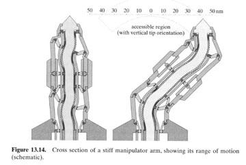
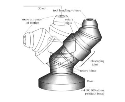
One of the first questions we’ll need to answer is: what does a molecular-scale positional device look like? Current proposals are similar to macroscopic robotic devices but on a much smaller scale. The illustrations (from Nanosystems, the best technical introduction to Nanotechnology) show a design for a molecular-scale robotic arm proposed by Eric Drexler, a pioneering researcher in the field.
Only 100 nanometers high and 30 nanometers in diameter, this rather squat design has a few million atoms and roughly a hundred moving parts. It uses no lubricants, for at this scale a lubricant molecule is more like a piece of grit. Instead, the bearings are “run dry” (following a suggestion by Feynman) as described in the following paragraph.
Running bearings dry should work both because the diamond surface is very slippery (see the coefficient of friction for diamond in the table) and because we can make the surface very smooth–so smooth that there wouldn’t even be molecular-sized asperities or imperfections that might catch or grind against each other. Computer models support our intuition: analysis of the bearings shown here using computational chemistry programs shows they should rotate easily.
Stiffness
Our molecular arms will be buffeted by something we don’t worry about at the macroscopic scale: thermal noise. This makes molecular-scale objects wiggle and jiggle, just as Brownian motion makes small dust particles bounce around at random. Can our molecular robotic arm maintain its position in the face of thermal noise?
The critical property we need here is stiffness. Stiffness is a measure of how far something moves when you push on it. If it moves a lot when you push on it a little, it’s not very stiff. If it doesn’t budge when you push hard, it’s very stiff.
Big positional devices, used in today’s Scanning Probe Microscopes (SPMs), have been made stiff enough to image individual atoms despite thermal noise. In SPMs, a very sharp tip is brought down to the surface of the sample being scanned. Like a blind man tapping in front of him with his cane, we can tell that the tip is approaching the surface and so can “feel” the outlines of the surface in front of us.
Many different types of physical interactions with the surface are used to detect its presence. Some scanning probe microscopes literally push on the surface–and note how hard the surface pushes back. Others connect the surface and probe to a voltage source, and measure the current flow when the probe gets close to the surface. A host of other probe-surface interactions can be measured, and are used to make different types of SPMs. But in all of them, the basic idea is the same: when the sharp tip of the probe approaches the surface a signal is generated–a signal which lets us map out the surface being probed.
The SPM can not only map a surface, in many cases the probe-surface interaction changes the surface as well. This has already been used experimentally to spell out molecular words, and the obvious opportunities to modify the surface in a controlled way are being investigated both experimentally and theoretically.
A few big SPMs making a few molecular structures won’t let us make much–certainly not tons of precisely structured shatterproof diamond. We’ll need vast numbers of very small positional devices operating in parallel. Unfortunately, as we make our positional devices smaller and smaller, they will be more and more subject to thermal noise. To make something that’s both small and stiff is more challenging. It helps to get the stiffest material you can find. Diamond, as usual, is stiffer than almost anything else and is an excellent material from which to make a very small, very stiff positional device. Theoretical analysis gives firm support to the idea that positional devices in the 100 nanometer size range able to position their tips to within a small fraction of an atomic diameter in the face of thermal noise at room temperature should be feasible. Trillions of such devices would occupy little more than a few cubic millimeters (a speck slightly larger than a pinhead).
Stewart Platforms
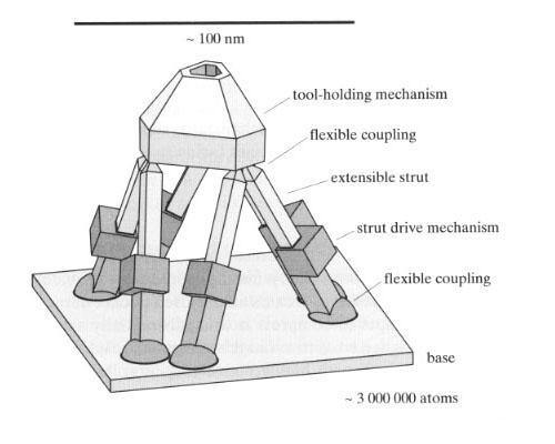
While Drexler’s proposal for a small robotic arm is easy to understand and should be adequate to the task, more recent work has focused on the Stewart platform. This positional device has the great advantage that it is stiffer than a robotic arm of similar size.
Conceptually, the Stewart platform is based on the observation that a polyhedron, all of whose faces are triangular, will be rigid. If some of the edges of the polyhedron can be adjusted in length, then the position of one face can be moved with respect to the position of another face. If we want a full six degrees of freedom (X, Y, Z, roll, pitch and yaw) then we must be able to independently adjust the lengths of six different edges of the polyhedron.
If we further want one triangular face of the polyhedron to remain of fixed size and hold a “tool,” and a second face of the polyhedron to act as the “base” whose size and position is fixed, then we find that the simplest polyhedron that will suit our purpose is the octahedron.
In the Stewart platform, one triangular face of the octahedron is designated the “platform,” while the opposing triangular face is designated the “base.” The six edges that connect the base to the platform can then be adjusted in length to control the position of the platform with respect to the base. Mechanically, this adjustment is often done using six hydraulic pistons. A picture of the Stewart platform (from Nanosystems) is shown above.
The advantage of the Stewart platform can now be seen: because the six adjustable-length edges are either in pure compression or pure tension and are never subjected to any bending force, this positional device is stiffer than a long robotic arm which can bend and flex. The Stewart platform is also conceptually simpler than a robotic arm, having fewer different types of parts; for this reason, we can reasonably expect that making one will be simpler than making a robotic arm.
The Utility of Diamond: Why It’s a Dream Material
From airplanes and space ships to cars and chairs, making products lighter and stronger is almost always an improvement. Sometimes, as in the case of space flight, this is a quantum leap all by itself. At other times it’s just a convenience: moving heavy furniture is a chore most of us would avoid if we could.
The strength and lightness of materials depends on the number and strength of the bonds that hold their atoms together, and the lightness of those atoms. Light atoms that form many strong bonds are at the heart of strong, light stiff materials. Boron, carbon and nitrogen are lighter and form more and stronger bonds than other atoms. The carbon-carbon bond in particular is very strong, and carbon atoms can form four bonds to four neighboring atoms. In diamond, this makes a very dense network of very strong bonds, which creates a very strong, light and stiff material. Besides light weight and great strength, diamond has a host of materials properties that make it an excellent choice for almost any application. (See the table for a list of diamond’s material properties).
| Source: Crystallume | ||
| Diamond’s Material Properties | Diamond’s Value | Comments |
| Chemical reactivity | Extremely low | |
| Hardness (kg/mm2) | 9000 | CBN: 4500 SiC: 4000 |
| Thermal conductivity (W/cm-K) | 20 | Ag: 4.3 Cu: 4.0 |
| Tensile strength (pascals) | 3.5 x 10⁹(natural) | 1011(theoretical) |
| Compressive strength (pascals) | 1011(natural) | 5 x 10¹¹(theoretical) |
| Band gap (ev) | 5.5 | Si: 1.1 GaAs: 1.4 |
| Resistivity (W-cm) | 1016 (natural) | |
| Density (gm/cm3) | 3.51 | |
| Thermal Expansion Coeff (K-1) | 0.8 x 10⁻⁶ | SiO2: 0.5 x 10⁻⁶ |
| Refractive index | 2.41 at 590 nm | Glass: 1.4 – 1.8 |
| Coeff. of Friction | 0.05 (dry, varies) | Teflon: 0.05 |
| Hole mobility(cm2/V-s) | 1600 | Si: 600 |
| Electron mobility (cm2/V-s) | 1900 | Si: 1500 |
| Breakdown voltage (V/cm) | greater than 107 | Si: 5 x 10⁶ |
Another material with remarkable properties is graphite: carbon atoms arranged in a hexagonal lattice with each carbon atom having three bonds to its three neighbors. While graphite has fewer bonds per atom, the strength of these bonds is greater and so graphitic materials also have remarkable properties.
Diamond is also a wonderful material for making transistors and computer gates, though it takes a bit of explanation to understand why.
Computer gates should switch as quickly as possible: that’s what makes computers so fast. To do this, the gates must be made of transistors in which the electrons move as fast as possible over the shortest possible distances. But as electrons move through a material, they generate heat: think of how hot the tungsten wire in a light bulb can get! So the faster we make our computer the faster the electrons move through the material and the hotter it gets. When it gets too hot the computer stops working.
Diamond excels in its electronic properties. Fundamentally, it lets us move charge around much faster before things stop working. There are several reasons for this. First, diamond transistors can operate at much higher temperatures because diamond has a larger “bandgap” than other materials (particularly silicon). Electrons in semiconductors (such as diamond or silicon) are either in the “conduction band” or the “valence band.” An electron in the conduction band can move freely and transport charge.
Moving an electron from the valence band to the conduction band requires adding a specific amount of energy to the electron. In silicon, this is 1.12 electron volts. In diamond, it is 5.47 electron volts. As the temperature increases, more and more electrons can jump into the conduction band from the valence band because of thermal noise. When too many electrons do this the semiconductor becomes conductive everywhere and the transistors short out and stop working. Because diamond has a wider bandgap, it shorts out at a proportionally higher temperature than silicon.
Diamond also has greater thermal conductivity, which lets us move heat out of a diamond transistor more quickly to prevent it from getting too hot.
To move an electron faster we want to “pull” on it harder. The stronger the electric field, the harder we’re pulling the electrons. But as the electric field gets too strong, it tears electrons out of the valence band causing the transistors to short out. This “breakdown” field varies from material to material, and (you guessed it) diamond leads the pack.
Finally, electrons (and holes) move with different speeds through different materials, even when the electric field is the same. Again, electrons and holes in diamond move faster than in silicon.
Because diamond transistors can be hotter, are more easily cooled, can tolerate higher voltages before breaking down, and electrons move more easily in them; they make better transistors than other materials. Diamond would be ideal for electronic devices if only we could manufacture it inexpensively and with precisely the desired structure.
In summary: from cars to airplanes to spaceships, from furniture to buildings, from pocket calculators to supercomputers, materials similar to diamond are just better than other materials, often a lot better. Just as the stone age, the bronze age and the steel age were named after the materials that we could make, this new age we are entering might be called the diamond age.
Positional Control and the Synthesis of Diamond
We can in principle make a great many very useful structures from diamond, including very powerful computers and molecular robotic devices able to position molecular components to within a fraction of an atomic diameter.
But how can we synthesize diamond? One answer to this question comes from looking at how we grow diamond today using Chemical Vapor Deposition (CVD). In a process somewhat reminiscent of spray painting, we build up layer after layer of diamond on a surface by holding that surface in a cloud of very reactive molecules and atoms–like H; CH3, C2H, etc. When these reactive molecules bump into the surface they change it, either by adding, removing, or re-arranging atoms. By carefully controlling the pressure, temperature, and the exact composition of the gas, we can create conditions that favor the growth of diamond on the surface.
While these are the right chemical reactions to make diamond, randomly bombarding the growing surface with reactive molecules doesn’t offer the finest control over the growth process. It would be like trying to build a wristwatch using a sandblaster. We want the chemical reactions to take place at precisely the places on the surface that we specify–not wherever random gusts of turbulent gas might dictate.
A second problem is that the hydrogenated diamond surface is chemically inert: it’s difficult to add carbon (or anything else) to it. We could overcome this problem by removing a hydrogen atom from the surface, leaving behind a very reactive dangling bond. This is a critical first step during CVD diamond growth but it happens at random, anywhere on the growing diamond surface, when the right kind of reactive gas molecule happens to strike the surface in the right way. We want to do something similar but more controlled: remove a specific hydrogen atom from a specific spot on the diamond surface. To do this, we’ll need a “hydrogen abstraction tool”.
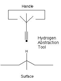
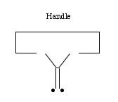
What might such a tool look like? If we base it on our understanding of diamond CVD, it should be a highly reactive radical with a high affinity for hydrogen. At the same time it must be possible to position it, so it must have a stable region which can serve as a “handle.” The tool would be held by (for example) the molecular robotic arm discussed earlier, and would be positioned directly over the hydrogen we wish to abstract.
A simple strategy for finding such radicals is to look through the table of bond strengths in the Handbook of Chemistry and Physics and pick the molecule with the strongest bond to hydrogen. The radical created by removing the hydrogen should then have a very high affinity for hydrogen, as desired. Unfortunately, this strategy first produces fluorine.
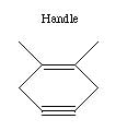
While atomic fluorine does indeed have a very high affinity for hydrogen, there is no obvious way to attach a “handle” to it. Interest therefore turns to the molecule with the second strongest bond to hydrogen: acetylene. Here, we are in luck. Not only does the acetylene radical have a high affinity for hydrogen, it also has a chemically stable region which can be modified into a “handle” (see illustration above).
Drexler realized this sometime in the early 1980’s. The author subsequently and independently followed the same line of logic and reached the same conclusions. An initial check of the validity of this idea was provided by semi-empirical calculations at Xerox PARC (easily done on a workstation using freely available programs). Discussions with Bill Goddard and members of his molecular modeling group at Caltech resulted in more accurate calculations using high level ab initio quantum chemistry methods on a more powerful computer. (These methods have the interesting property that the calculations will converge on the correct answer if enough computing power is used).
Drexler published this observation in Nanosystems in 1992. A group at NRL interested in diamond growth found the proposal intriguing and modeled the abstraction of a hydrogen at room temperature using a qualitatively different computational model of molecular behavior (which permitted them to model the behavior of several hundreds of atoms in the vicinty of the abstraction).
As the results of three different computational approaches have all produced the same qualitative answer, and as the results are also in accord with our intuition about what should happen, it’s safe to say that this hydrogen abstraction tool will, when finally implemented, be able to abstract hydrogen.
The hydrogen abstraction tool illustrates some important ideas common to other proposals for molecular tools for the synthesis of diamond. First, the tool has a reactive end which is brought into contact with the molecular workpiece and an inert end which is held by a molecular positional device. Second, the point of application of the tool is controlled by the molecular positional device. Third, the environment around the tool is itself inert (typical proposals involve the use of either vacuum or a noble gas). The inert environment prevents the tool (which is quite reactive) from reacting with anything undesired.
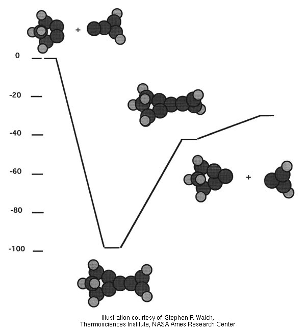
While the hydrogen abstraction tool creates a very reactive spot on the surface we also need a tool that will deposit one or more carbon atoms on the growing surface. One proposal is the dimer deposition tool. (a “dimer” is just two of something stuck together. In this case, two carbon atoms are stuck together by a triple bond, hence the two carbon atoms form a “dimer”).
A dimer deposition tool is simply a dimer with two weak bonds to a supporting structure. A proposal by Drexler is shown to the left. A second proposed dimer deposition tool, which has particularly weak bonds to the dimer, is illustrated at the right. [Subsequent note: further investigation of the proposal at right suggests it might not be stable except at very low temperatures. A variety of alternative dimer deposition tools are possible, so even if this particular structure should prove unsastisfactory for room temperature operation, other tools able to carry out the same function should be feasible.]
To illustrate how we might combine the use of the hydrogen abstraction tool with the dimer deposition tool, we proceed in three steps. First, we start with the hydrogenated diamond (111) surface. (The notation (111) refers to a particular surface of the diamond crystal. When diamond shatters, it shatters along certain planes and not along others. As these different planes have surfaces with different properties, it’s important to specify which plane you’re talking about). Second, we use the hydrogen abstraction tool to remove two adjacent hydrogen atoms. Third, we use the dimer deposition tool to deposit two carbon atoms on the surface–the two ends of the carbon dimer are originally single-bonded to the rest of the tool.
The two dangling bonds on the surface are very reactive, and react with the ends of the carbon dimer. When this happens, the bonds holding the dimer to the dimer deposition tool break, and the bonds in the deposition tool rearrange to eliminate what would otherwise be two radicals. Result: the carbon dimer is transferred from the tool to the surface.
The following illustration shows the dimer deposition tool adding a dimer to a small cluster which represents the diamond (111) surface. (Because accurate ab initio calculations are computationally less expensive for a small cluster of atoms, the following illustrations show only the atoms directly involved in the reaction).
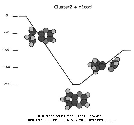
This sequence of steps starts with a flat diamond surface and adds two carbon atoms to it. It could be repeated at other sites. A computational investigation of the final step was reported by Stephen Walch at the recent workshop on computational Nanotechnology sponsored by the program at NASA. Because the energy released during the reaction is much larger than thermal noise (e.g., the reaction is quite exothermic), the reverse reaction is very unlikely to occur.
The barrier to the reaction is also small. Taken together, these mean the reaction can take place easily and irreversibly. The dimer will “snap” onto the surface and stay there. (Calculations at the 6-31G* MP2 level show all positive vibrational frequencies for this tool. Further investigation of its stability is in progress).
A third proposed tool is the carbene insertion tool. “It is no exaggeration to claim a major role for carbenes in the modern chemists’s attitude that he can very probably make anything he wants.” (W. J. Baron). A positionally controlled carbene should be correspondingly more useful, as it could be made to react at any position on a growing molecular workpiece. Carbenes are very reactive and can insert readily into double and triple bonds. A plausible reaction would be to insert a carbene into the dimer described above.
This is illustrated in the following figure. (Some intermediates in the reaction pathway have been omitted for clarity).
A fourth proposal is for a hydrogen deposition tool. Where the hydrogen abstraction tool is intended to make an inert structure reactive by creating a dangling bond, the hydrogen deposition tool would do exactly the opposite: make a reactive structure inert by terminating dangling bonds. This tool could be used during the synthetic process to stabilize a structure that might otherwise undergo a spontaneous and undesired rearrangement or reconstruction, or it could be used at the end of the synthetic process to stabilize the finished product.
There are many possible candidates for such a tool: any molecular structure that has a weak bond to a hydrogen. One particularly attractive candidate is the use of tin. The hydrogen-tin bond is quite weak, and so a tin-based hydrogen deposition tool should be quite effective.
These four tools let us (a) make an inert surface reactive by removing a hydrogen from one or more specific sites, (b) add one or two carbon atoms to a surface at selected sites and (c) make a reactive surface inert by adding hydrogen to it–which lets us prevent undesired surface rearrangements.
The Stiff Hydrocarbons as a Model System for Study
These four molecular tools–by themselves–should be sufficient to make a remarkably wide range of stiff hydrocarbons. This suggests that we define a simplified model of nanotechnology that we might call “hydrocarbon-based nanotechnology.” This simplified version would only be able to make things from hydrogen and carbon–a much less ambitious goal than making things from the approximately 100 elements found in the full periodic table.
But in exchange for confining ourselves to this more limited class of structures, we make it much easier to analyze the structures that can be fabricated and the synthetic reactions needed to make them. This narrower proposal can be more readily and more thoroughly investigated than full nanotechnology.
At the same time, hydrocarbon-based nanotechnology retains several of the key features of general nanotechnology. Diamond and shatterproof variants of diamond still fall within its purview; and it can still make all the parts needed for the operation of basically mechanical devices, including: struts, bearings, gears, robotic arms, and the like.
It’s often useful to define a somewhat broader class than the stiff hydrocarbons, but a class which is still much more restrictive than the class of “most structures consistent with physical law.” We’d like to be able to build molecular structures that are similar to diamond but which incorporate some other elements. We might want to add impurities (as in diamond electronic devices) or terminate a bearing surface with fluorine. Perhaps we’re bending the diamond structure, and want to add some silicon internally to relieve the strain, (the silicon-carbon bond is longer than the carbon-carbon bond, so adding silicon to a region will “puff it up”). Or we find that adding some nitrogen to the internal surface of a bearing will relieve some strain (the nitogen-carbon bond is slightly shorter than the carbon-carbon bond).
The term “diamondoid” is used to cover these (and related) possiblities. Diamondoid materials are made primarily of the elements hydrogen; first row elements like carbon, nitrogen, oxygen or fluorine; and second row elements like silicon, phosphorous, sulfur or chlorine; all held together by many strong covalent bonds. While including only about a tenth of the elements in the periodic table, the diamondoid materials include many structures of striking utility.
Self-Replication: Making Things Inexpensively
Positional control combined with appropriate molecular tools should let us build a truly staggering range of molecular structures–but a few molecular devices built at great expense would hardly seem to qualify as a revolution in manufacturing. How can we keep the costs down?
Potatoes are a miracle of biology with tens of thousands of genes and proteins and intricate molecular machinery; yet we think nothing of eating this miracle, mashed with a little butter. Potatoes, along with many other agricultural products, cost less than a dollar a pound. The key reason: provide them with a little dirt, water and sunlight and a potato can make more potatoes.
If we could make a general purpose programmable manufacturing device which was able to make copies of itself (the author does work at Xerox, after all….), then the manufacturing costs for both the devices and anything they made could be kept quite low–likely no more than the costs for growing potatoes. Drexler called such devices “assemblers.”
The first serious analysis of self replicating systems was by von Neumann in the 1940’s. He carried out a detailed analysis of one such system in a theoretical cellular automata model (The best known example of a cellular automata model is Conway’s Game of Life, which is played out on a giant checkerboard and uses a simple set of rules to decide what happens at each square of the checkerboard at each time step).
In von Neumann’s cellular automata model he used a universal computer for control and a “universal constructor” to build more automata. The “universal constructor” was a robotic arm that, under computer control, could move in two dimensions and alter the state of the cell at the tip of its arm. By sweeping systematically back and forth, the arm could “build” any structure that the computer instructed it to. In his three-dimensional “kinematic” model, von Neumann retained the idea of a positional device (now able to position in three dimensions rather than two) and a computer to control it.
A NASA study in 1980 extended the general conclusions of von Neumann and concluded that a fully automated lunar mining and manufacturing operation, able to extend itself using its own mining and manufacturing capabilities, would be feasible and could be built given a multi-billion dollar budget and a few decades of work. (Note that this kind of budget and time frame was in keeping with other proposed aerospace projects of the time).
The architecture for Drexler’s assembler is a specialization of the more general architecture proposed by von Neumann. As before, there is a computer and constructor, but now the computer has shrunk to a “molecular computer” while the constructor combines two features: a robotic positional device (such as the robotic arm discussed earlier) and a well defined set of chemical operations that take place at the tip of the positional device (such as the hydrogen abstraction reaction and the other reactions involved in the synthesis of diamond).
The complexity of a self replicating system need not be excessive. In this context the complexity is just the size, in bytes, of a “recipe” that fully describes how to make the system. The complexity of an assembler needn’t be beyond the complexity that can be dealt with by today’s engineering capabilities. As shown in the following table, there are several self replicating systems whose complexity is well within current capabilities. Drexler estimated the complexity of his original proposal for an assembler at about 10,000,000 bytes. Further work should reduce this.
| Von Neumann’s Universal Constructor | about 60,000 |
| Internet worm | 60,000 |
| Mycoplasma capricolum | 200,000 |
| E. Coli | 1,000,000 |
| Drexler’s Assembler | 12,000,000 |
| Human | 800,000,000 |
| NASA Lunar Manufacturing Facility | over 10,000,000,000 |
What is the “complexity” of a living system? We’ll take this to mean the number of bytes in the DNA “blueprints.” As each base pair in DNA can be one of four possibilities, it encodes two bits. One byte (8 bits) can be encoded in four base pairs. This means we count the number of base pairs in the DNA and divide by four to get the number of bytes in the “blueprints.”
For Mycoplasma capricolum, which has around 800,000 base pairs, this results in about 200,000 bytes. For humans, with roughly 3.2 billion base pairs, this results in 800 million bytes. (We’re using the haploid base pair count: each cell in your body has DNA from your mother and DNA from your father–but much of this is similar. We’re counting only the DNA from one parent). The complexity and sophistication of most living systems goes well beyond anything we might need just to achieve low cost manufacturing. Much of the complexity of the human genome is unrelated to issues of self-replication: people do more than just self-replicate!
The complexity of the Internet worm is just an estimate of the number of bytes in its C program. Because the environment in which it operates is highly structured and provides relatively easy access to complex and sophisticated software, it could be argued that its complexity might be much less than the complexity of a system that operated in a “simple” environment. We’ll leave it in our table anyway, as it’s an interesting data point.
This argument is less applicable to von Neumann’s universal constructor which operates in a simple environment: just a large two-dimensional checkerboard with a finite number of states at each square. Its complexity is an estimate of the number of bytes needed to describe the constructor. The complexity of the NASA Lunar Manufacturing Facility was estimated in the NASA study.
What Will We Be Able To Make?
Today, most airplanes are made from metal despite the fact that diamond has a strength-to-weight ratio over 50 times that of aerospace aluminum. Diamond is expensive, we can’t make it in the shapes we want, and it shatters. Nanotechnology will let us inexpensively make shatterproof diamond (with a structure that might resemble diamond fibers) in exactly the shapes we want. This would let us make a Boeing 747 whose unloaded weight was 50 times lighter but just as strong.
Today, travel in space is very expensive and reserved for an elite few. Nanotechnology will dramatically reduce the costs and increase the capabilities of space ships and space flight. The strength-to-weight ratio and the cost of components are absolutely critical to the performance and economy of space ships: with nanotechnology, both of these parameters will be improved by one to two orders of magnitude. Improvements in these two parameters alone (ignoring other advantages provided by nanotechnology) should improve the overall cost/performance ratio by over three orders of magnitude.
This has led the National Space Society (NSS) to adopt a position paper supporting nanotechnology; Dan Goldin, NASA’s chief administrator, to support nanotechnology; and NAS at NASA Ames Research Center to start a project (now with perhaps half a dozen researchers) to examine molecular manufacturing systems and molecular machines using computational models.
Beyond inexpensively providing remarkably light and strong materials for space ships, nanotechnology will also provide extremely powerful computers with which to guide both those ships and a wide range of other activities in space.
Today, computer chips are made using lithography–literally “stone writing.” It’s our finest manufacturing technology, but there seem to be fundamental limits in how much further we can improve it. In lithography, we draw fine lines on a silicon wafer by using methods borrowed from photography. A light-sensitive film–called a “resist”–is spread over the silicon wafer. The resist is exposed to a complex pattern of light and dark, like a negative in a camera, and developed. The exposed resist is then washed away, and a particular chemical is sprayed over the surface. Where the resist has been washed away, the chemical reaches the surface of the silicon and can diffuse a short distance into it. Where the resist has not been washed away, the spray is blocked.
Finally, the remaining resist is washed away, along with any chemicals that it prevented from reaching the silicon surface. The result: a fine pattern of some desired chemical is laid out on the silicon surface. By repeating this process, an intricate set of interlocking patterns can be made that defines the complex logic elements of a modern computer chip.
If the computer hardware revolution is to continue at its current pace, in a decade or so we’ll have to move beyond lithography to some new post lithographic manufacturing technology. Making patterns on a resist and spraying chemicals around simply can’t arrange atoms with the ultimate precision that should be feasible. More precise methods will be needed.
Ultimately, each logic element will be made from just a few atoms. Designs for computer gates with less than 1,000 atoms have already been proposed–but each atom in such a small device has to be in exactly the right place. To economically build and interconnect trillions upon trillions of such small and precise devices in a complex three dimensional pattern we’ll need a manufacturing technology well beyond today’s lithography: we’ll need nanotechnology. With it, we should be able to build mass storage devices that can store more than a hundred billion billion bytes in a volume the size of a sugar cube; RAM that can store a mere billion billion bytes in such a volume; and massively parallel computers of the same size that can deliver a billion billion instructions per second.
Today, “smart” weapons are fairly big–we have the “smart bomb” but not the “smart bullet.” In the future, even weapons as small as a single bullet could pack more computer power than the largest supercomputer in existence today, allowing them to perform realtime image analysis of their surroundings and communicate with weapons tracking systems to acquire and navigate to targets with greater precision and control. We’ll also be able to build weapons both inexpensively and much more rapidly, at the same time taking full advantage of the remarkable materials properties of diamond. Rapid and inexpensive manufacture of great quantities of stronger more precise weapons guided by massively increased computational power will alter the way we fight wars. Changes of this magnitude could destabilize existing power structures in unpredictable ways.
Military applications of nanotechnology raise a number of concerns that prudence suggests we begin to investigate before, rather than after, we develop this new technology. While molecular manufacturing will not arrive for many years, its obvious military potential will increasingly attract the interest of strategic planners.
For example, in a talk titled Nanotechnology and global security at the Fourth Foresight Conference on Molecular Nanotechnology, Admiral David E. Jeremiah, USN (Ret), former Vice Chairman of the Joint Chiefs of Staff, said “Military applications of molecular manufacturing have even greater potential than nuclear weapons to radically change the balance of power.” As it seems implausible that military applications of this technology will never be developed and deployed, it would seem safer to encourage the relatively early interest of those organizations less prone to the abuse of power and more likely to curb its abuse by others.
To make power today we dig coal and oil from the ground, we dam rivers, and we burn nuclear fuel in nuclear power plants. Yet the sunshine all around us could provide orders of magnitude more power than we use–and do so more cleanly and less expensively–if only we could make low cost solar cells and batteries. We already know how to make solar cells that are efficient enough for this application: it just costs too much to make them.
Nanotechnology will cut costs both of the solar cells and the equipment needed to deploy them, making solar power economical. In this application we need not make new or technically superior solar cells: making inexpensively what we already know how to make expensively would move solar power into the mainstream.
Today, our surgical tools are large and crude at the molecular scale–yet the cellular and molecular machinery in our tissue is small and precise. There is a fundamental mismatch between the capabilities of our tools and what’s needed to cure the injuries in our tissue. Today’s scalpels are, as seen by a cell, large crude scythes that are more suited to cut and tear than to heal and mend. Ripping through tissue, they leave dead and maimed cells in their wake. The only reason that modern surgery works is the remarkable ability of cells to regroup, bury their dead, and heal over the wound.
It is not modern medicine that does the healing, but the cells themselves: we are but onlookers. If we had surgical tools that were molecular both in their size and precision, we could develop a medical technology that for the first time would let us directly heal the injuries at the molecular and cellular level that are the root causes of disease and ill health. With the precision of drugs combined with the intelligent guidance of the surgeon’s scalpel, we can expect a quantum leap in our medical capabilities.
Nanotechnology should let us make almost every manufactured product faster, lighter, stronger, smarter, safer and cleaner. We can already see many of the possibilities as these few examples illustrate. New products that solve new problems in new ways are more difficult to foresee, yet their impact is likely to be even greater. Could Edison have foreseen the computer, or Newton the communications satellite?
Summary of the Core Technology
We can now see the fundamental shape of a molecular manufacturing technology. Self replicating assemblers, operating under computer control, let us inexpensively build more assemblers. The assemblers can be reprogrammed to build other products. The assemblers use programmable positional control to position molecular tools and molecular components, permitting the inexpensive fabrication of most structures consistent with physical law. Diamondoid materials in particular become inexpensive and commonplace, and their remarkable properties usher in what has been called the Diamond Age.
Developmental Pathways
In the preceding discussion of nanotechnology we gave scant attention to possible developmental pathways that would let us migrate from our current technology to what we might call “mature” systems able to inexpensively manufacture most diamondoid structures. The proposals advanced so far have been driven largely by the desired goal: a system able to inexpensively synthesize most diamondoid structures. The proposal that emerged was a general purpose programmable manufacturing system which uses positionally controlled highly reactive tools in vacuum and is able to self replicate.
No constraint was imposed requiring that the proposed system be easy to fabricate given our current technology–and indeed, this problem appears non trivial. But we must eventually build such systems if they are to be of any use–how can we do this? To give the reader some feeling for the magnitude of the effort involved, we can compare the requirements for a mature system with present capabilities.
A mature system must be able to build an assembler with hundreds of millions or billions of atoms with no atom out of place. If we are to do this, and if each unit operation typically handles one or a few atoms (a hydrogen abstraction, a carbene insertion, etc), then either the error rate per unit operation must be low (less than one in a billion) or we must adopt error detection and correction methods.
A general rule of thumb is that making something right the first time is easier than making it wrong and fixing it. Given the choice between a manufacturing process that has a low enough error rate that most finished products will simply work correctly the first time versus a process which requires elaborate error detection and correction to make any working products at all, the former is greatly to be preferred.
Because analysis of the fundamental causes of errors during the manufacture of diamondoid products in general and assemblers in particular supports the idea that error rates substantially lower than one in a billion should be achievable, and hence that an assembler can make another assembler with a high probability of success while using no error detection or correction, existing design proposals adopt the simpler and higher performance approach.
Had the opposite conclusion been reached, i.e., that error rates could not be driven below one in one billion, then design proposals would have adopted a smaller module size (consistent with the error rate) and incorporated appropriate mechanisms for module testing, the rejection of bad modules, and the assembly of working modules into larger systems.
This line of logic results in proposals for assemblers in which error rates are very low. These low error rates, however, are predicated on the prior existence of diamondoid assemblers. Unfortunately, we do not have assemblers today. Worse, current technology would be hard pressed to achieve such error rates. Chemists view a synthesis that provides 99% yield as very good. The synthesis of proteins from amino acids by ribosomes has an error rate of perhaps one in 10,000.
Replication of DNA, by using extensive error detection and correction, along with built in redundancy (DNA has two complementary strands), achieves an error rate of roughly one base in a billion (which varies depending on particular circumstances).
The size of structure that can be built by today’s SPMs without error is smaller than has been achieved by chemists. The first such work arranged 35 xenon atoms on a nickel surface at 4 kelvins in vacuum to spell out ” IBM.” Later work in Japan spelled out “NANO SPACE” at room temperature in vacuum by removing individual sulfur atoms from the surface. More recently, 6 molecules were arranged in a hexagonal pattern at room temperature in vacuum.
As each molecule had 173 atoms, this modular approach was able to position over 1,000 atoms. While these are great successes we have not yet seen a long sentence spelled out in this fashion, let alone a paragraph or a book. Further, SPMs can “see” the structure that’s being built. Current successes use this ability to provide constant feedback to the human operator, who can detect and correct errors.
In short, today’s SPMs can build structures that are only a small fraction of the size of proposed assemblers and have error rates high enough that they must use relatively sophisticated error detection and correction methods.
The situation is made more difficult by the additional requirement that unit operations be fast. If an assembler is to manufacture a copy of itself in about a day, and if this takes one hundred million to a billion operations, then each unit operation must take place in a fraction of a millisecond. Ribosomes take tens of milliseconds to add a single amino acid to a growing protein. Today’s SPMs can take hours to arrange a few atoms or molecules.
At the same time, the use of vacuum prevents us from using self assembly or any of the other solution-based techniques developed by chemistry. Abandoning these powerful tools does not seem like a good first step.
While speed, reliability and operation in vacuum do not pose fundamental problems, the conclusion is obvious: directly building a diamondoid assembler using existing technology is a daunting task. Perhaps, rather than attempting to solve all the problems in a single giant leap, we should instead approach them in a more incremental fashion. To this end, we need to define one or more intermediate systems. Almost by definition, an intermediate system is easier to build from current technology, but is still able to make systems that are more powerful than itself. A series of intermediate systems, each able to build the next system in the chain, would let us adopt more incremental methods.
One approach is to eliminate the requirement that the assembler be made from diamondoid structures. We wanted to make diamondoid structures because of their remarkable strength, stiffness, electrical properties, etc. But an intermediate system need only be able to make a more advanced system, and perhaps products that are impressive in comparison with today’s products. It doesn’t have to be diamondoid itself.
This suggests what might be called “building block based nanotechnology.” Rather than building diamond, we’ll build some other material from molecular building blocks that are relatively large: tens, hundreds or even thousands of atoms in size. Larger building blocks reduce the number of assembly steps, so fewer unit operations are needed and they need not be as reliable. Soluble building blocks, with “linkage” groups that are selective (the building blocks only stick to other building blocks, not to the solvent or low concentrations of contaminants) eliminate the need for vacuum.
We certainly have many choices: any of the wide range of molecules that chemists have synthesized or could reasonably synthesize which has the desired properties. Krummenacker concluded that each molecular building block should have at least three sites where it can link to other building blocks (two sites leads to the familiar polymers so ubiquitous in biological systems: proteins, DNA, RNA, etc. Addition of a third site makes the design of three dimensional stiff structures much easier).
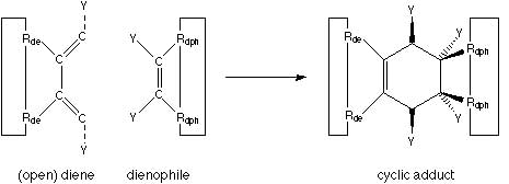
While such building blocks could be linked to each other using any one of a variety of reactions, a particularly attractive possibility is the Diels-Alder reaction. This reaction, well known to chemists, works in most solvents (or even in vacuum). It involves a reaction between a diene and a dieneophile. The reaction is specific: the diene and the dieneophile react with each other but seldom with other groups (see illustration above, courtesy of Krummenacker).
Because it works in vacuum and doesn’t produce any small molecules (which would destroy the vacuum), it could be used both in intermediate systems in solution, and later in systems that use vacuum to make diamondoid materials.
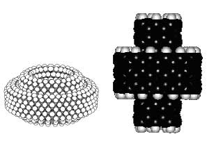
Solution based systems could use positional control to assemble the building blocks, but can also use the methods of self assembly. In particular, the self assembly of a positional device should be feasible. If you ask someone familiar with the field if it would be feasible to self assemble a robotic arm, the usual response is some variation of “no.” If, instead, you ask whether it would be feasible to self assemble an octahedron, the usual response is to point out that Nadrian Seeman of New York University has already self assembled a truncated octahedron from DNA and plans to do the same for a regular octahedron (both for reasons unrelated to positional control). (The computer generated graphic of the truncated octahedron at right is courtesy of Nadrian Seeman). For this work he received The 1995 Feynman Prize in nanotechnology.
As we have seen, an octahedron is the basic structure required for the Stewart platform. The truncated octahedron, because it has sides that aren’t triangular, is floppier than a regular octahedron. Even the regular octahedron is likely to be too floppy for this application because of the limited stiffness of DNA. Further, the length of the edges cannot be changed (a requirement if we wish to control the position of the platform with respect to the base).
However, self assembling a Stewart platform able to assemble molecular building blocks seems much less difficult than directly building a diamondoid assembler able to synthesize diamond in vacuum. Several ways to deal with the problem of inadequate stiffness and adjustable length edges are possible.
One way would be to attach selectively sticky strands of DNA to a stiff molecular structure. This would let us use DNA (which has been intensively studied and whose selective stickiness is well known) to guide the process of self assembly, while the stiff molecular structure would would let us deal with concerns about inadequate stiffness. To change the length of an edge, we would need to use molecular structures that change shape in response to light, pressure, temperature, chemicals, or some other external signal.
Many such molecular structures are known. Self assembling a Stewart platform whose edges are stiff enough to make a useful positional device, and the length of whose edges can be changed by a suitable signaling mechanism, is no longer a challenge that seems beyond our reach.
A second approach for positioning molecular building blocks in solution is to use an Atomic Force Microscope (AFM). This type of SPM relies on “touch” to create an image. By pushing on the structure being scanned, and feeling how hard it pushes back, the AFM can build up an image of stiff structures (it doesn’t work very well when the applied force is strong enough to deform the structure). Because the AFM touches the surface of the structure being probed, it can also change that surface. To do this, it’s very useful if the precise molecular structure of the tip can be controlled, so that the precise nature of the tip-surface interaction can be well defined.
This line of reasoning leads to the “molecular manipulator:” an AFM with a reactive fragment of an antibody bound to its tip. By changing the antibody, we can change what type of molecule will stick to the AFM tip. If the antibody both sticks selectively to a particular molecular building block, and also is bound to the AFM tip, we can now position the molecular building block by positioning the AFM tip. We can use any one of a wide range of possible molecular building blocks (antibodies can today be created that will bind to most small molecules). Again, this no longer seems beyond our reach.
Another developmental pathway is defined by the desire of the semiconductor industry to make ever smaller transistors despite the fact that optical lithography–the current workhorse manufacturing method for making computer chips–will reach a limit in a few more years. Transistors are made today by “drawing” very fine lines on silicon–but the optical methods in use today are limited by the wavelength of light: a few hundred nanometers. SPMs could let us make much smaller circuits by drawing much finer lines.
Already demonstrated for making the finest and most critical lines in a transistor, if this approach can be made low cost and reliable it would let the entire semiconductor industry be retooled to use these finer lines to make more and smaller transistors. This, by itself, is not molecular nanotechnology; but once we learn to draw the smallest and finest lines of all, lines where every atom is in the right place (and there will be strong economic incentives to move in this direction), we could use the same techniques to make molecular machines.
At first, these molecular machines would be very expensive and useful only for applications where their remarkable precision would justify the cost–but they should eventually lead to machines sophisticated enough to make simple assemblers.
Whether through self-assembly, by improvements in SPMs, some hybrid approach, or perhaps by some other path; we are moving from an era of expensive and imprecise products to an era of inexpensive products of molecular precision. We are going to replace most of the manufacturing base of the world with a fundamentally new and much better manufacturing technology.
The Critics
Arguments that nanotechnology is infeasible are relatively rare and uniformly poor in technical quality. The best known are the arguments of David Jones, a Nature columnist and chemist. Quoted extensively in a Scientific American article on nanotechnology (see http://www.foresight.org/SciAmDebate/SciAmOverview.html for commentary) he advanced arguments like the following: “Single atoms … are amazingly mobile and reactive. They will combine instantly with ambient air, water, each other, the fluid supporting the assemblers, or the assemblers themselves.”
However, as the proposals involving reactive molecular tools specify that the environment should be inert (i.e., vacuum) there is no “ambient air” to react with. As the molecular tools are positionally controlled, they will not react with each other or the assembler itself for the same reason that a hot soldering iron does not react with the skin of the person doing the soldering.
Jones’ criticisms raise greater questions about his understanding of the field than about the feasibility of nanotechnology. Other arguments against the feasibility of nanotechnology have likewise had obvious flaws, reminiscent of the 1920 New York Times editorial which said that rockets to the moon were impossible because there was no air to push against in space.
As should be clear from this article there are major technical challenges that must be overcome if we are to develop molecular manufacturing systems able to synthesize diamondoid structures. The serious questions, however, are about which development pathways should be pursued and how long it will take.
How Long?
The single most frequently asked question about nanotechnology is: how long?. How long before it will let us make molecular computers? How long before inexpensive solar cells let us use clean solar power instead of oil, coal, and nuclear fuel? How long before we can explore space at a reasonable cost?
The scientifically correct answer is: I don’t know.
Having said that, it is worth pointing out that the trends in the development of computer hardware have been remarkably steady for the last 50 years. Such parameters as
- the number of atoms required to store one bit
- the size of a transistor
- the energy dissipated by a single logic operation
- the resolution of the finest machining technology
- the cost of a computer gate
have all declined with great regularity, even as the underlying technology has changed dramatically. From relays to vacuum tubes to transistors to integrated circuits to Very Large Scale Integrated circuits (VLSI) we have seen steady declines in the size and cost of logic elements and steady increases in their performance.
Extrapolation of these trends suggests we will have to develop molecular manufacturing in the 2010 to 2020 time frame if we are to keep the computer hardware revolution on schedule.
Of course, extrapolating past trends is a philosophically debatable method of technology forecasting. While no fundamental law of nature prevents us from developing nanotechnology on this schedule (or even faster), there is equally no law that says this schedule will not slip.
Much worse, though, is that such trends imply that there is some ordained schedule–that nanotechnology will appear regardless of what we do or don’t do. Nothing could be further from the truth. How long it takes to develop this technology depends very much on what we do. If we pursue it systematically, it will happen sooner. If we ignore it, or simply hope that someone will stumble over it, it will take much longer. And by using theoretical, computational and experimental approaches together, we can reach the goal more quickly and reliably than by using any single approach alone.
While some advances are made through serendipitous accidents or a flash of insight, others require more work. It seems unlikely that a scientist would forget to turn off the bunsen burner in his lab one afternoon and return to find he’d accidentally made a Space Shuttle.
Like the first human landing on the moon, the Manhattan project or the development of the modern computer the development of molecular manufacturing will require the coordinated efforts of many people for many years. How long will it take? A lot depends on when we start.