Korean researchers grow wafer-scale graphene on a silicon substrate
July 21, 2015

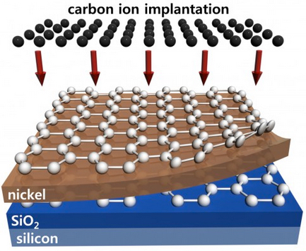
Wafer-scale (4 inch in diameter) synthesis of multi-layer graphene using high-temperature carbon ion implantation on nickel/SiO2/silicon (credit: J.Kim/Korea University, Korea)
Taking graphene a step closer to realistic commercial applications in silicon microelectronics, Korea University researchers have developed a simple microelectronics-compatible method for growing multi-layer graphene on a high-quality, wafer-scale (four inches in diameter) silicon substrate.
The method is based on the ion implantation technique — a process in which ions are accelerated under an electrical field and smashed into a semiconductor. The impacting ions change the physical, chemical, or electrical properties of the semiconductor.
Because of its high conductivity, “graphene is a potential contact electrode and an interconnection material linking semiconductor devices to form the desired electrical circuits, explained Jihyun Kim, the team leader and a professor in the Department of Chemical and Biological Engineering at Korea University.
However, “to deposit large-area graphene that is free of wrinkles, tears, and residues on silicon wafers requires low temperatures. That can’t be achieved with conventional chemical vapor deposition, which requires a high growth temperature — above 1,000 degrees Celsius.” That can cause strains, metal spiking, cracks, wrinkles, and contaminants from diffusion of dopants.
“Our synthesis method is controllable and scalable, allowing us to obtain graphene as large as the size of the silicon wafer,” Kim said. The researchers’ next step is to further lower the temperature in the synthesis process and to control the thickness of the graphene for manufacturing production.
The research is described in an open-access paper published this week in the journal Applied Physics Letters.
Abstract of Wafer-scale synthesis of multi-layer graphene by high-temperature carbon ion implantation
We report on the synthesis of wafer-scale (4 in. in diameter) high-quality multi-layer graphene using high-temperature carbon ion implantation on thin Ni films on a substrate of SiO2/Si.Carbon ions were bombarded at 20 keV and a dose of 1 × 1015 cm−2 onto the surface of the Ni/SiO2/Si substrate at a temperature of 500 °C. This was followed by high-temperature activation annealing (600–900 °C) to form a sp2-bonded honeycomb structure. The effects of post-implantation activation annealing conditions were systematically investigated by micro-Raman spectroscopy and transmission electron microscopy. Carbon ion implantation at elevated temperatures allowed a lower activation annealing temperature for fabricating large-area graphene. Our results indicate that carbon-ion implantation provides a facile and direct route for integrating graphene with Si microelectronics.