Looking deeper into semiconductors to create faster, smaller electronics
October 25, 2012

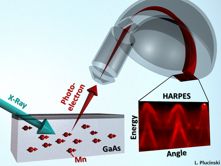
The new hard X-ray angle-resolved photoemission spectroscopy technique lets UC Davis researchers look inside new materials and study their properties (credit: Lukasz Plucinski, Peter Grunberg Institute)
University of California, Davis researchers for the first time have looked inside gallium manganese arsenide, which could open up an entirely new class of faster, smaller devices based on an emerging field known as “spintronics.”
Materials of this type might be used to read and write digital information not by using the electron’s charge, as is the case with today’s electronic devices, but by using its “spin.”
Understanding the magnetic behavior of atoms is key to designing spintronics materials that could operate at room temperature, an essential property for real-world applications.
The new study used a novel technique, hard X-ray angle-resolved photoemission spectroscopy (HARPES), developed by Charles Fadley, distinguished professor of physics at UC Davis and the Lawrence Berkeley National Lab, and recent UC Davis doctoral graduate Alexander Gray, together with colleagues at LBNL and in Germany and Japan.
The research represents the first major application of the HARPES technique, which was first described in a proof-of-principle paper by Gray, Fadley and colleagues last year.
Angle-resolved photoemission spectroscopy uses Einstein’s famous photoelectric effect to study materials. If you bombard atoms with light particles — photons — you knock out electrons, known as photoelectrons, which fly out at precise angles, energies and spins depending on the structure of the material.
For many years, researchers have used “soft” or low-energy X-rays as the photon source, but that technique can look only at the top nanometer of a material — about five atoms deep. Fadley and Gray developed a method that uses “hard” (high-energy) X-rays to look much deeper inside a material, to a depth of about 40 to 50 atoms.
The researchers selected gallium manganese arsenide because it’s a widely used semiconductor. Add a few percent of manganese atoms to the mix, and in the right conditions — a temperature below 170 Kelvin (about 150 degrees below zero Fahrenheit) for one — and it becomes ferromagnetic like iron, with all of the individual manganese atomic magnets lined up in the same direction. Physicists call this class of materials dilute magnetic semiconductors.
There were two competing ideas to explain how gallium manganese arsenide becomes magnetic at certain temperatures. The HARPES study shows that, in fact, both mechanisms contribute to the magnetic properties.
“We now have a better fundamental understanding of electronic interactions in dilute magnetic semiconductors that can suggest future materials,” Fadley said. “HARPES should provide an important tool for characterizing these and many other materials in the future.”
Gray and Fadley conducted the study at the SPring-8 synchrotron radiation facility, operated by the Japanese National Institute for Materials Sciences. New HARPES studies are now under way at LBNL’s Advanced Light Source synchrotron.
The work was supported by grants from the U.S. Department of Energy and the governments of Japan and Germany.