Miniaturized camera chip provides superfine depth resolution for 3D printing
April 6, 2015

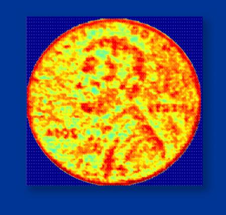
A 3D image produced by the new NCI chip. The image, taken from roughly half a meter (1.5 feet) away, shows an angled side view of the penny. (credit: Ali Hajimiri/Caltech)
Imagine you need to have a precise copy of an object. You take a snapshot with your smartphone, send it to your 3D printer, and within minutes you have a replica accurate to within microns of the remote original object.
That’s what a tiny new high-resolution 3D imager developed at Caltech called a “nanophotonic coherent imager” (NCI) could achieve in the future.
The NCI provides the highest depth-measurement accuracy of any such nanophotonic 3D imaging device, using an inexpensive silicon chip less than a millimeter square in size, says Ali Hajimiri, the Thomas G. Myers Professor of Electrical Engineering in the Caltech Division of Engineering and Applied Science, who heads the research.
While 3D imaging systems are available, the most sensitive ones are too large and expensive to be used in consumer applications.
How it works
In a regular camera, each pixel represents the intensity of the light received from a specific point in the image, which could be near or far from the camera — meaning that the pixels provide no information about the relative distance of the object from the camera.
In contrast, each pixel in an image created by the NCI provides both distance and intensity information. “Each pixel on the chip is an independent interferometer — an instrument that uses the interference of light waves to make precise measurements — which detects the phase and frequency of the signal in addition to the intensity,” says Hajimiri.
Caltech | New Camera Chip Enables Micrometer-Resolution 3D Images
A LIDAR array
The new chip uses an established detection and ranging technology called LIDAR (Laser Illuminated Detection And Ranging), used in autonomous vehicles, for example. With LIDAR, a target object is illuminated with scanning laser beams. The reflected light is then analyzed to provide information about the object’s size and its distance from the laser to create an image of its surroundings.
However. the new camera chip has an entire array of tiny LIDARs on a coherent imager, so “we can simultaneously image different parts of an object or a scene without the need for any mechanical movements within the imager,” Hajimiri says.
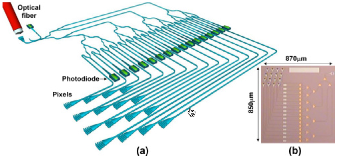
The device uses an optical concept known as coherence. If two light waves are coherent, the waves have the same frequency, and the peaks and troughs of light waves are exactly aligned with one another. In the NCI, the object is illuminated with this coherent light. The light that is reflected off of the object is then picked up by on-chip detectors, called grating couplers, that serve as “pixels,” because the light detected from each coupler represents one pixel on the 3D image.

The structure of the 4 × 4 NCI, in which the light coming from the object is collected using 16 grating couplers (pixels) is shown. A fraction of the coherent light that is used to illuminate the object is guided using an optical fiber and is coupled into the chip through a grating coupler. This coupled light is combined with the collected optical signals from the object and is photo-detected using on-chip silicon-germanium photodiodes. (b) The NCI micro-photograph implemented on standard IME silicon-on-insulator process. (credit: Firooz Aflatouni et al./Optics Express)
On the NCI chip, the phase, frequency, and intensity of the reflected light from different points on the object is detected and used to determine the exact distance of the target point.
Because the coherent light has a consistent frequency and wavelength, it is used as a reference with which to measure the differences in the reflected light. In this way, the NCI uses the coherent light as sort of a very precise ruler to measure the size of the object and the distance of each point on the object from the camera. The light is then converted into an electrical signal that contains intensity and distance information for each pixel — all of the information needed to create a 3D image.
Highest level of depth accuracy in silicon photonics
The incorporation of coherent light allows 3D imaging with the highest level of depth-measurement accuracy ever achieved in silicon photonics, says Hajimiri. It also makes it possible for the device to fit in a very small size.
“By coupling, confining, and processing the reflected light in small pipes on a silicon chip, we were able to scale each LIDAR element down to just a couple of hundred microns [millionths of a meter] in size — small enough that we can form an array of 16 of these coherent detectors on an active area of 300 microns by 300 microns.”
The first proof of concept of the NCI has only 16 coherent pixels, meaning that the 3D images it produces can only be 16 pixels at any given instance. However, the researchers also developed a method for imaging larger objects by first imaging a four-pixel-by-four-pixel section, then moving the object in four-pixel increments to image the next section.
With this method, the team used the device to scan and create a 3D image of the “hills and valleys” on the front face of a U.S. penny — with micron-level resolution — from half a meter away.
Superfine visual accuracy for driveless cars
Hajimiri says the current array of 16 pixels could also be easily scaled up to hundreds of thousands. One day, by creating such vast arrays of these tiny LIDARs, the imager could be applied to a broad range of applications from very precise 3D scanning and printing to helping driverless cars avoid collisions to improving motion sensitivity in superfine human machine interfaces, where the slightest movements of a patient’s eyes and the most minute changes in a patient’s heartbeat can be detected on the fly.
“The small size and high quality of this new chip-based imager will result in significant cost reductions, which will enable thousands new of uses for such systems by incorporating them into personal devices such as smartphones,” he says.
The study was published in an open-access paper in Optics Express and was partially funded by Caltech Innovation Initiative.
Abstract of Nanophotonic coherent imager
An integrated silicon nanophotonic coherent imager (NCI), with a 4 × 4 array of coherent pixels is reported. In the proposed NCI, on-chip optical processing determines the intensity and depth of each point on the imaged object based on the instantaneous phase and amplitude of the optical wave incident on each pixel. The NCI operates based on a modified time-domain frequency modulated continuous wave (FMCW) ranging scheme, where concurrent time-domain measurements of both period and the zero-crossing time of each electrical output of the nanophotonic chip allows the NCI to overcome the traditional resolution limits of frequency domain detection. The detection of both intensity and relative delay enables applications such as high-resolution 3D reflective and transmissive imaging as well as index contrast imaging. We demonstrate 3D imaging with 15μm depth resolution and 50μm lateral resolution (limited by the pixel spacing) at up to 0.5-meter range. The reported NCI is also capable of detecting a 1% equivalent refractive index contrast at 1mm thickness.