Molybdenum disulfide as an alternative to graphene
April 7, 2014

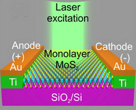
Schematic diagram of the MoS2 monolayer photosensor, showing electrical connections and laser photo-excitation (credit: Néstor Perea-López et al./2D Materials)
Molybdenum disulfide (MoS2) has been put forward by a group of researchers as a potential building block for the next generation of low-cost electrical devices as an alternative to graphene.
Because of its impressive ability to convert light into electricity at with high efficiency, single layers of the semiconducting material have been used to fabricate a widely used device known as a photosensor, which is found in a range of appliances from solar panels and digital cameras to remote controls.
The device is featured in an article (open access) in the first issue of IOP Publishing’s new journal 2D Materials — a multidisciplinary journal with a focus on applications and fundamental science concerning all aspects of graphene and 2D materials.
Bottom-up production in bulk
In their study, the researchers highlighted the suitability of MoS2 by successfully demonstrating the photosensor’s ability to efficiently convert the energy from photons (delivered to the device at two separate wavelengths by a laser) into an electric current.
“The thinnest foil of MoS2 has a thickness of three atoms,” said lead author of the research, Nestor Perea-Lopez, from The Pennsylvania State University. “One can picture this monolayer foil as a sandwich, where sulfur atoms are the bread and molybdenum is the ham. [Because of the thin monolayer form], it can convert photons into electrons very efficiently, making it an ideal material to use in light detectors, such as the ones used in digital cameras.”
But a significant challenge that remains for researchers working with 2D materials is how to produce the materials in bulk. Graphene, for example, can only be produced in bulk through a liquid phase or by exfoliating (peeling off) graphite into very thin layers or flakes, which can be very difficult to control.
The goal is to be able to synthesize 2D materials using a bottom-up approach instead, carefully piecing individual components together like building blocks.
The researchers did this successfully in their study by growing tiny triangles of single-layered MoS2, around five microns wide onto a silica-based substrate, using a bottom-up process known as chemical vapour deposition (shown in illustration).
“The devices we built are very small which means that we could integrate millions in a few millimeter squares,” said Perea-Lopez.
“Graphene is a semi-metal, which means that electrons can move through the material very fast even with very small voltages,” he said, but that means graphene devices can be hard to turn off, unlike MoS2, with has a large energy gap that allows it to have very large on/off ratios of hundreds of millions.
“Not everything about graphene is wrong though, and the path in this field must be the integration of metals and semi-metals, such as graphene, with insulators such as boron nitride and semiconductors like MoS2 to create the next generation of devices.”
* MoS2 is part of a wider group of materials known as transition metal dichalcogenides.
Abstract of 2D Materials paper
We report the fabrication of a photosensor based on as-grown single crystal monolayers of MoS2 synthesized by chemical vapor deposition (CVD). The measurements were performed using Au/Ti leads in a two terminal configuration on CVD-grown MoS2 on a SiO2/Si substrate. The device was operated in air at room temperature at low bias voltages ranging from −2 V to 2 V and its sensing capabilities were tested for two different excitation wavelengths (514.5 nm and 488 nm). The responsivity reached 1.1 mA W−1 when excited with a 514.5 nm laser at a bias of 1.5 V. This responsivity is one order of magnitude larger than that reported from photo devices fabricated using CVD-grown multilayered WS2. A rectifying-effect was observed for the optically excited current, which was four times larger in the direct polarization bias when compared to the reverse bias photocurrent. Such rectifying behavior can be attributed to the asymmetric electrode placement on the triangular MoS2 monocrystal. It is envisioned that these components could eventually be used as efficient and low cost photosensors based on CVD-grown transition metal dichalcogenide monolayers.