New electron microscopy method sculpts 3-D structures with one-nanometer features
November 10, 2015

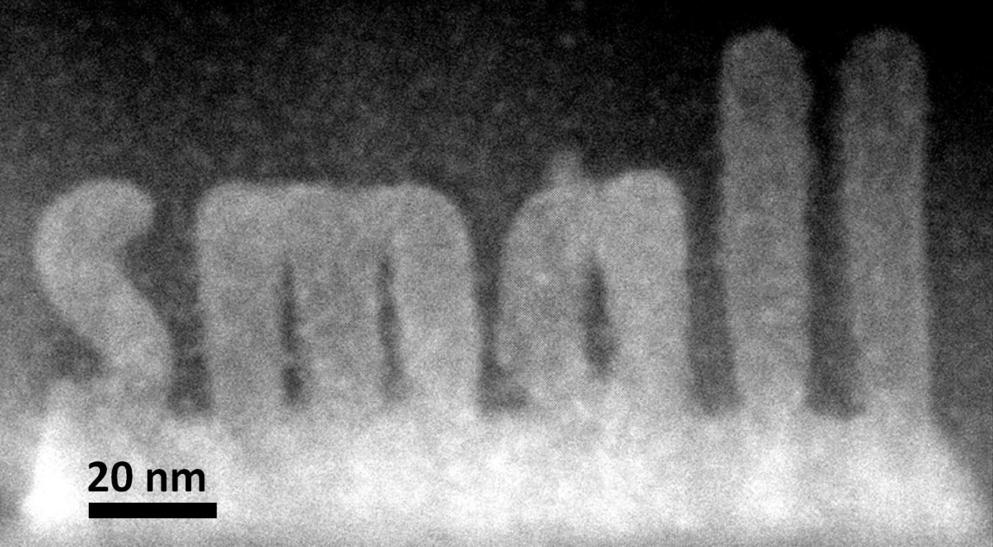
ORNL researchers used a new scanning transmission electron microscopy technique to sculpt 3-D nanoscale features in a complex oxide material. (credit: Department of Energy’s Oak Ridge National Laboratory)
Oak Ridge National Laboratory researchers have developed a way to build precision-sculpted 3-D strontium titanate nanostructures as small as one nanometer, using scanning transmission electron microscopes, which are normally used for imaging.
The technique could find uses in fabricating structures for functional nanoscale devices such as microchips. The structures grow epitaxially (in perfect crystalline alignment), which ensures that the same electrical and mechanical properties extend throughout the whole material, with more pronounced control over properties. The process can also be observed with atomic resolution.
The use of a scanning transmission electron microscope, which passes an electron beam through a bulk material, sets the approach apart from lithography techniques, which only pattern or manipulate a material’s surface. Combined with electron beam path control, the process could lead to large-scale implementation of bulk atomic-level fabrication as a new enabling tool of nanoscience and technology, providing a bottom-up, atomic-level complement to 3D printing, the researchers say.
“We’re using fine control of the beam to build something inside the solid itself,” said ORNL’s Stephen Jesse. “We’re making transformations that are buried deep within the structure. It would be like tunneling inside a mountain to build a house.”
The technique also offers a shortcut to researchers interested in studying how materials’ characteristics change with thickness. Instead of imaging multiple samples of varying widths, scientists could use the microscopy method to add layers to the sample and simultaneously observe what happens.
The study is published in the journal Small.
Abstract of Atomic-Level Sculpting of Crystalline Oxides: Toward Bulk Nanofabrication with Single Atomic Plane Precision
The atomic-level sculpting of 3D crystalline oxide nanostructures from metastable amorphous films in a scanning transmission electron microscope (STEM) is demonstrated. Strontium titanate nanostructures grow epitaxially from the crystalline substrate following the beam path. This method can be used for fabricating crystalline structures as small as 1–2 nm and the process can be observed in situ with atomic resolution. The fabrication of arbitrary shape structures via control of the position and scan speed of the electron beam is further demonstrated. Combined with broad availability of the atomic resolved electron microscopy platforms, these observations suggest the feasibility of large scale implementation of bulk atomic-level fabrication as a new enabling tool of nanoscience and technology, providing a bottom-up, atomic-level complement to 3D printing.