New kind of ‘tandem’ solar cell developed
March 26, 2015
Test sample of a monolithic perovskite-silicon multijunction solar cell produced by the MIT-Stanford University team (credit: Felice Frankel)
Researchers at MIT and Stanford University have developed a new kind of solar cell that combines two different layers of sunlight-absorbing material to harvest a broader range of the sun’s energy. The development could lead to photovoltaic cells that are more efficient than those currently used in solar-power installations, the researchers say.
The new cell uses a layer of silicon — which forms the basis for most of today’s solar panels — but adds a semi-transparent layer of a material called perovskite*, which can absorb higher-energy particles of light. Unlike an earlier “tandem” solar cell reported by members of the same team earlier this year — in which the two layers were physically stacked, but each had its own separate electrical connections — the new version has both layers connected together as a single device that needs only one control circuit.
The new findings are reported in the open-access paper in the journal Applied Physics Letters by MIT graduate student Jonathan Mailoa; associate professor of mechanical engineering Tonio Buonassisi; Colin Bailie and Michael McGehee at Stanford; and four others.
Simpler to make and install
“Different layers absorb different portions of the sunlight,” Mailoa explains. In the earlier tandem solar cell, the two layers of photovoltaic material could be operated independently of each other and required their own wiring and control circuits, allowing each cell to be tuned independently for optimal performance.

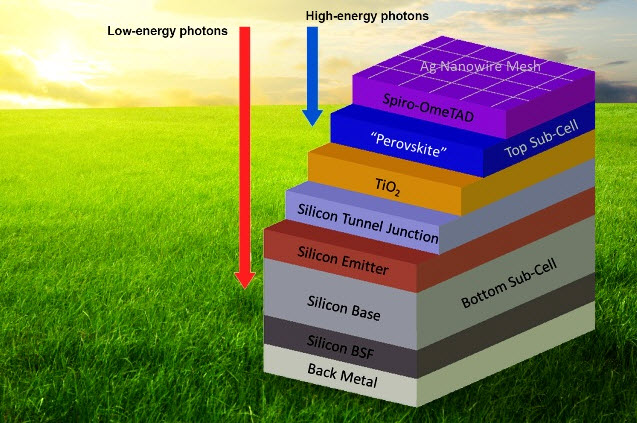
Schematic diagram shows the layered structure of the hybrid solar cell. The top sub-cell, made of pervoskite (blue), absorbs most of the high-energy (blue arrow) photons from the sun, while letting lower energy (red arrow) photons pass through, where they are absorbed by the lower sub-cell made of silicon (gray). The other layers serve to provide electrical connections between the two sub-cells, and to carry the electricity generated by the cells out to wires where it can be harnessed. (credit: Jose-Luis Olivares/MIT)
By contrast, the new combined version should be much simpler to make and install, Mailoa says. “It has advantages in terms of simplicity, because it looks and operates just like a single silicon cell,” he says, with only a single electrical control circuit needed.
Perovskites have been studied for potential electronic uses including solar cells, but this is the first time they have been successfully paired with silicon cells in this configuration, a feat that posed numerous technical challenges.
Increased efficiency

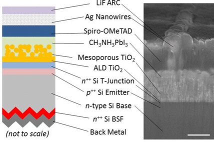
The device structure of a 2-terminal monolithically grown perovskite/Si multijunction solar cell with an n-type silicon base. The polished SEM image is taken at 45° tilt to show the silver nanowire mesh (500 nm scale bar). (credit: Jonathan P. Mailoa et al./Appl. Phys. Lett.)
Now the team is focusing on increasing the power efficiency — the percentage of sunlight’s energy that gets converted to electricity — that is possible from the combined cell. In this initial version, the efficiency is 13.7 percent, but the researchers say they have identified low-cost ways of improving this to about 30 percent — a substantial improvement over today’s commercial silicon-based solar cells — and they say this technology could ultimately achieve a power efficiency of more than 35 percent.
They will also explore how to easily manufacture the new type of device, but Buonassisi says that should be relatively straightforward, since the materials lend themselves to being made through methods very similar to conventional silicon-cell manufacturing.
One hurdle is making the material durable enough to be commercially viable: The perovskite material degrades quickly in open air, so it either needs to be modified to improve its inherent durability or encapsulated to prevent exposure to air — without adding significantly to manufacturing costs and without degrading performance.
The research was supported by the Bay Area Photovoltaic Consortium and the U.S. Department of Energy.
* As KurzweilAI has noted, the versatile perovskite material has also been used for harvesting hydrogen fuel from sunlight and water at lower cost, in lower-cost high-brightness LEDs, as an infrared superlens, and in future chips that operate at atomic dimensions.
Abstract of A 2-terminal perovskite/silicon multijunction solar cell enabled by a silicon tunnel junction
With the advent of efficient high-bandgap metal-halide perovskite photovoltaics, an opportunity exists to make perovskite/silicon tandem solar cells. We fabricate a monolithic tandem by developing a silicon-based interband tunnel junction that facilitates majority-carrier charge recombination between the perovskite and silicon sub-cells. We demonstrate a 1 cm2 2-terminal monolithic perovskite/silicon multijunction solar cell with a V OC as high as 1.65 V. We achieve a stable 13.7% power conversion efficiency with the perovskite as the current-limiting sub-cell, and identify key challenges for this device architecture to reach efficiencies over 25%.