New solid-state memory technology allows for highest-density non-volatile storage
August 10, 2015

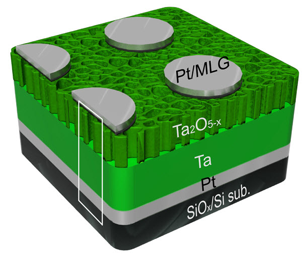
A schematic shows the layered structure of new type of solid-state memory developed at Rice University (credit: Tour Group/Rice University)
Scientists in the Rice University lab of chemist James Tour have created a solid-state memory technology that allows for high-density 162 gigabits nonvolatile storage, much higher than other oxide-based memory systems under investigation by scientists. (Eight bits equal one byte; a 162-gigabit unit would store about 20 gigabytes of information.)
Applying voltage to a 250-nanometer-thick sandwich of graphene, tantalum, nanoporous tantalum oxide (an insulator), and platinum creates addressable bits where the layers meet. Control voltages shift oxygen ions and vacancies to switch the bits between ones and zeroes.
Like the Tour lab’s previous discovery of silicon oxide memories, the new devices require only two electrodes per circuit, making them simpler than present-day flash memories, which use three. “This is a new way to make ultradense, nonvolatile computer memory,” Tour said.
Nonvolatile random-access memories, such as such as flash memory in smartphones and tablets, hold their data even when the power is off, unlike volatile random-access computer memories (in most computers), which lose their contents when the machine is shut down.
Modern memory chips have many requirements: They have to read and write data at high speed and hold as much as possible. They must also be durable and show good retention of that data while using minimal power. These are provided by Rice’s new design, which requires only one hundredth the amount of energy required with present devices, Tour says.
“This tantalum memory is based on two-terminal systems, so it’s all set for 3-D memory stacks,” he said. “And it doesn’t even need diodes or selectors, making it one of the easiest ultradense memories to construct. This will be a real competitor for the growing memory demands in high-definition video storage and server arrays.”

A layered structure of tantalum, tantalum oxide, multilayer graphene, and platinum is the basis for a new type of nonvolatile memory (credit: Tour Group/Rice University)
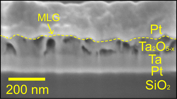
In making the material, the researchers found the tantalum oxide gradually loses oxygen ions, changing from an oxygen-rich, nanoporous semiconductor at the top to oxygen-poor at the bottom. Where the oxygen disappears completely, it becomes pure tantalum, a metal. The graphene does double duty as a barrier that keeps platinum from migrating into the tantalum oxide and causing a short circuit.*
Rice University | Tantalum oxide memory: Slices taken from a tantalum oxide-based memory developed at Rice University show the partially interconnected and randomly distributed internal pores in the material.
Tour said tantalum oxide memories can be fabricated at room temperature. He noted the control voltage that writes and rewrites the bits is adjustable, which allows a wide range of switching characteristics.
(As the researchers note in a paper in the journal Nano Letters, nonvolatile resistive oxide-based memories can also offer faster switching speed. That suggests that tantalum oxide memories might one day further improve MIT’s “BlueDBM” solution for improved handling of big data by making nonvolatile memory more efficient, as described on KurzweilAI last week.)
The remaining hurdles to commercialization of tantalum oxide memories include the fabrication of a dense enough crossbar device to address individual bits and a way to control the size of the nanopores.
The research is described online in the American Chemical Society Researchers at Korea University-Korea Institute of Science and Technology and University of Massachusetts, Amherst where also involved.
Tour is the T.T. and W.F. Chao Chair in Chemistry as well as a professor of materials science and nanoengineering and of computer science and a member of Rice’s Richard E. Smalley Institute for Nanoscale Science and Technology.
Rice University | Tantalum oxide memory 2
* The researchers determined three related factors give the memories their unique switching ability:
- The control voltage mediates how electrons pass through a boundary that can flip from an ohmic (current flows in both directions) to a Schottky (current flows one way) contact and back.
- The boundary’s location can change based on oxygen vacancies. These are “holes” in atomic arrays where oxygen ions should exist, but don’t. The voltage-controlled movement of oxygen vacancies shifts the boundary from the tantalum/tantalum oxide interface to the tantalum oxide/graphene interface. “The exchange of contact barriers causes the bipolar switching,” said Gunuk Wang, lead author of the study and a former postdoctoral researcher at Rice.
- The flow of current draws oxygen ions from the tantalum oxide nanopores and stabilizes them. These negatively charged ions produce an electric field that effectively serves as a diode to hinder error-causing crosstalk. While researchers already knew the potential value of tantalum oxide for memories, such arrays have been limited to about a kilobyte because denser memories suffer from crosstalk that allows bits to be misread.
Abstract of Three-Dimensional Networked Nanoporous Ta2O5–x Memory System for Ultrahigh Density Storage
Oxide-based resistive memory systems have high near-term promise for use in nonvolatile memory. Here we introduce a memory system employing a three-dimensional (3D) networked nanoporous (NP) Ta2O5–x structure and graphene for ultrahigh density storage. The devices exhibit a self-embedded highly nonlinear I–V switching behavior with an extremely low leakage current (on the order of pA) and good endurance. Calculations indicated that this memory architecture could be scaled up to a ∼162 Gbit crossbar array without the need for selectors or diodes normally used in crossbar arrays. In addition, we demonstrate that the voltage point for a minimum current is systematically controlled by the applied set voltage, thereby offering a broad range of switching characteristics. The potential switching mechanism is suggested based upon the transformation from Schottky to Ohmic-like contacts, and vice versa, depending on the movement of oxygen vacancies at the interfaces induced by the voltage polarity, and the formation of oxygen ions in the pores by the electric field.