Spot-welding a graphene nanoribbon to connect into a circuit
June 17, 2013

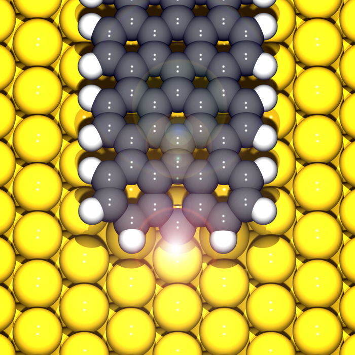
Contacting (connecting) a graphene nanoribbon (carbon atoms shown in gray and hydrogen in white) via a single chemical bond by removing a single hydrogen atom (bright area) (credit: Aalto University)
Scientists at Aalto University and Utrecht University have created single-atom contacts between gold and graphene nanoribbons.
The challenge for graphene devices has been how design a contact (to connect the graphene to a circuit wire) without affecting the performance of the graphene nanostructures.
Graphene is a single layer of carbon atoms arranged in a honeycomb lattice. It is anticipated to be a revolutionizing material for future electronics.
Graphene transistors functioning at room temperature are sized less than 10 nanometers. This means that the graphene nanostructures are only a few tens of atoms in width, requiring atomically precise electrical contacts.
So they used a single chemical bond to make an electrical contact to a graphene nanoribbon. To do that, they first used atomic force microscopy (AFM) and scanning tunneling microscopy (STM) to map the structure of the graphene nanoribbons with atomic resolution.
Then they used a voltage pulse from the tip of the scanning tunneling microscope to form a single bond to the graphene nanoribbon — at a specific atomic location. The pulse removes a single hydrogen atom from the end of a graphene nanoribbon and this initiates the bond formation.
Combining the microscopy experiments with theoretical modelling, the team developed a detailed picture of the contacted nanoribbon properties.
The most significant discovery is that a single chemical bond forms an electronically transparent contact with the graphene nanoribbon — without affecting its overall electronic structure. This may be the key to using graphene nanostructures in future electronic devices, as the contact does not change the intrinsic ribbon properties.
“Combined AFM and STM allows us to characterize the graphene nanostructures atom-by-atom, which is critical in understanding how the structure, the bonds with the contacts and their electrical properties are related,” explains Dr Ingmar Swart who leads the team concentrating on STM and AFM measurements at Utrecht University
The study was performed at Aalto University Department of Applied Physics and at the Debye Institute in Utrecht University. The groups at Aalto are part of the Academy of Finland’s Centres of Excellence in “Low Temperature Quantum Phenomena and Devices” and “Computational Nanosciences.” Academy of Finland and the European Research Council ERC funded the research.