Stamping out low-cost nanodevices
June 1, 2011
A simple technique for stamping patterns invisible to the human eye onto a special class of nanomaterials has been developed by researchers at Vanderbilt University.
The new method works with porous nanomaterials that are riddled with tiny voids, which give them unique optical, electrical, chemical, and mechanical properties. There are nanoporous forms of gold, silicon, alumina, and titanium oxide, among others.
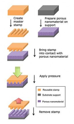
The technique involves the creation of pre-mastered stamps using traditional, but complex, clean room processes and then using the stamps to create patterns using a new process called direct imprinting of porous substrates (DIPS). DIPS can create a device in less than a minute, regardless of its complexity.
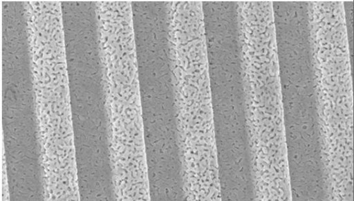
The smallest pattern the researchers have made to date has features of only a few tens of nanometers (about the size of a single fatty acid molecule). They have also succeeded in imprinting the smallest pattern yet reported in nanoporous gold, one with 70-nanometer features.
The first device the group has created is a “diffraction-based” biosensor that can be configured to identify a variety of different organic molecules, including DNA, proteins and viruses. The researchers envision a wide range of applications including drug delivery, chemical and biological sensors, solar cells, and battery electrodes.

Scanning electron microscope (SEM) image of a pattern directly imprinted in nanoporous gold (credit: Weiss Lab)
Judson D. Ryckman, Marco Liscidini, et al., Direct Imprinting of Porous Substrates: A Rapid and Low-Cost Approach for Patterning Porous Nanomaterials, Nano Letters, 2011; 11 (5): 1857 [DOI: 10.1021/nl1028073]
