This advance could finally make graphene-based semiconductor chips feasible
March 31, 2017

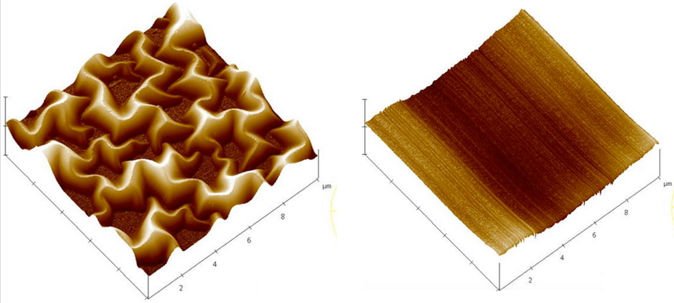
Atomic force microscopy images of as-deposited (left) and laser-annealed (right) reduced graphene oxide (rGO) thin films. The entire “pulsed laser annealing” process is done at room temperature and atmospheric pressure, using high-power laser pulses to convert p-type rGO material into n-type and completed in about one fifth of a microsecond. (credit: Anagh Bhaumik and Jagdish Narayan/Journal of Applied Physics)
Researchers at North Carolina State University (NC State) have developed a layered material that can be used to develop transistors based on graphene — a long-sought goal in the electronics industry.
Graphene has attractive properties, such as extremely high conductivity, meaning it conducts the flow of electrical current really well (compared to copper, for example), but it’s not a semiconductor, so it can’t work in a transistor (aside from providing great connections). A form of graphene called “graphene oxide” is a semiconductor, but it does not conduct well.
However, a form of graphene oxide called “reduced graphene oxide” (rGO) does conduct well*. Despite that, rGO still can’t function in a transistor. That’s because the design of a transistor is based on creating a junction between two materials: one that is positively charged (p-type) and one that is negatively charged (n-type), and native rGO is only a p-type.
The NC State researchers’ solution was to use high-powered laser pulses to disrupt chemical groups on an rGO thin film. This disruption moved electrons from one group to another, effectively converting p-type rGO to n-type rGO. They then used the two forms of rGO as two layers (a layer of n-type rGO on the surface and a layer of p-type rGO underneath) — creating a layered thin-film material that could be used to develop rGO-based transistors for use in future semiconductor chips.
The researchers were also able to integrate the rGO-based transistors onto sapphire and silicon wafers across the entire wafer.
The paper was published in the Journal of Applied Physics. The work was done with support from the National Science Foundation.
* Reduction is a chemical reaction that involves the gaining of electrons.
Abstract of Conversion of p to n-type reduced graphene oxide by laser annealing at room temperature and pressure
Physical properties of reduced graphene oxide (rGO) are strongly dependent on the ratio of sp2 to sp3hybridized carbon atoms and the presence of different functional groups in its structural framework. This research for the very first time illustrates successful wafer scale integration of graphene-related materials by a pulsed laser deposition technique, and controlled conversion of p to n-type 2D rGO by pulsed laser annealing using a nanosecond ArF excimer laser. Reduced graphene oxide is grown onto c-sapphire by employing pulsed laser deposition in a laser MBE chamber and is intrinsically p-type in nature. Subsequent laser annealing converts p into n-type rGO. The XRD, SEM, and Raman spectroscopy indicate the presence of large-area rGO onto c-sapphire having Raman-active vibrational modes: D, G, and 2D. High-resolution SEM and AFM reveal the morphology due to interfacial instability and formation of n-type rGO. Temperature-dependent resistance data of rGO thin films follow the Efros-Shklovskii variable-range-hopping model in the low-temperature region and Arrhenius conduction in the high-temperature regime. The photoluminescence spectra also reveal less intense and broader blue fluorescence spectra, indicating the presence of miniature sized sp2 domains in the vicinity of π* electronic states, which favor the VRH transport phenomena. The XPS results reveal a reduction of the rGO network after laser annealing with the C/O ratio measuring as high as 23% after laser-assisted reduction. The p to n-type conversion is due to the reduction of the rGO framework which also decreases the ratio of the intensity of the D peak to that of the G peak as it is evident from the Raman spectra. This wafer scale integration of rGO with c-sapphire and p to n-type conversion employing a laser annealing technique at room temperature and pressure will be useful for large-area electronic devices and will open a new frontier for further extensive research in graphene-based functionalized 2D materials.