A new way to make large sheets of graphene
May 28, 2014

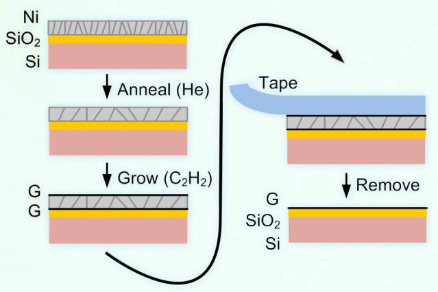
Illustrated here is a new process for making graphene directly on a nonmetal substrate. First, a nickel layer is applied to the material, in this case silicon dioxide (SiO2). Then carbon is deposited on the surface, where it forms layers of graphene above and beneath the SiO2. The top layer of graphene, attached to the nickel, easily peels away using tape (or, for industrial processes, a layer of adhesive material), leaving behind just the lower layer of graphene stuck to the substrate. (Credit: Daniel Q. McNerny et al.)
Researchers at MIT and the University of Michigan have developed a process that lends itself to making graphene directly on materials such as large sheets of glass.
Previous processes have used tiny flakes of graphene or graphene films on metal foil, with limited success.
The new process, described in a paper published in the journal Scientific Reports (open access), makes graphene on both the film’s top and bottom, using chemical vapor deposition (CVD).
The substrate is silicon dioxide, a form of glass, with a film of nickel on top. The nickel film can then be peeled away, leaving just the graphene on top of the nonmetallic substrate. This way, there’s no need for a separate process to attach the graphene to the intended substrate.
Christos Dimitrakopoulos, a professor of chemical engineering at the University of Massachusetts at Amherst who was not involved in this work, says, “This is a very significant piece of work for very large-area applications of graphene on insulating substrates.”
Compared to other methods, such as the use of a silicon carbide (SiC) substrate to grow graphene, he says, “The fact that the lateral size of graphene in the Hart group’s approach is limited only by the size of the [CVD] reactor, instead of the size of the SiC wafer, is a major advantage.”
The work was supported by Guardian Industries, the National Science Foundation, and the Air Force Office of Scientific Research.
Abstract of Scientific Reports paper
We demonstrate direct production of graphene on SiO2 by CVD growth of graphene at the interface between a Ni film and the SiO2 substrate, followed by dry mechanical delamination of the Ni using adhesive tape. This result is enabled by understanding of the competition between stress evolution and microstructure development upon annealing of the Ni prior to the graphene growth step. When the Ni film remains adherent after graphene growth, the balance between residual stress and adhesion governs the ability to mechanically remove the Ni after the CVD process. In this study the graphene on SiO2 comprises micron-scale domains, ranging from monolayer to multilayer. The graphene has >90% coverage across centimeter-scale dimensions, limited by the size of our CVD chamber. Further engineering of the Ni film microstructure and stress state could enable manufacturing of highly uniform interfacial graphene followed by clean mechanical delamination over practically indefinite dimensions. Moreover, our findings suggest that preferential adhesion can enable production of 2-D materials directly on application-relevant substrates. This is attractive compared to transfer methods, which can cause mechanical damage and leave residues behind.