A promising new 2-D semiconductor material
September 30, 2015

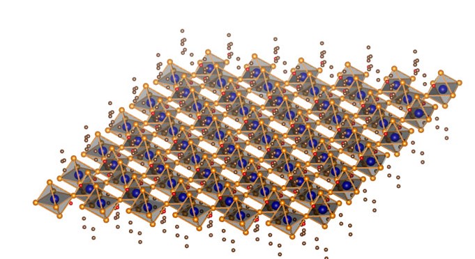
Ultrathin sheets of a new 2-D hybrid perovskite are square-shaped and relatively large in area, properties that should facilitate their integration into future electronic devices (credit: Peidong Yang, Berkeley Lab)
The first atomically thin 2D sheets of organic-inorganic hybrid perovskites have been created by Lawrence Berkeley National Laboratory (Berkeley Lab) researchers, adding to the growing list of two-dimensional semiconductors, such as graphene, boron nitride, and molybdenum disulfide, whose unique electronic properties make them potential successors to silicon in future devices.
However, unlike the other contenders, which are covalent semiconductors, these 2D hybrid perovskites are ionic materials, which gives them special properties of their own.
Traditional perovskites are typically metal-oxide materials that display a wide range of electromagnetic properties, including ferroelectricity and piezoelectricity, superconductivity and colossal magnetoresistance. As KurzweilAI has reported, perovskites have been solution-processed recently into thin films or bulk crystals for photovoltaic devices, reaching 20-percent power conversion efficiency; and have been used to create lower-cost, high-brightness LEDs.
2D atomically thin nanostructures
The new ultrathin sheets are of high quality, large in area, and square-shaped. They also exhibited efficient photoluminescence, color-tunability, and a unique structural relaxation not found in covalent semiconductor sheets.
“We believe this is the first example of 2D atomically thin nanostructures made from ionic materials,” says Peidong Yang, a chemist with Berkeley Lab’s Materials Sciences Division and world authority on nanostructures, who first came up with the idea for this research some 20 years ago.
“The results of our study open up opportunities for fundamental research on the synthesis and characterization of atomically thin 2D hybrid perovskites and introduce a new family of 2D solution-processed semiconductors for nanoscale optoelectronic devices, such as field effect transistors and photodetectors.”
Yang, who also holds appointments with the University of California (UC) Berkeley and is a co-director of the Kavli Energy NanoScience Institute (Kavli-ENSI), is the corresponding author of a paper describing this research in the journal Science.

Structural illustration of a single layer of a 2D hybrid perovskite (C4H9NH3)2PbBr4), an ionic material with different properties than 2D covalent semiconductors (credit: Peidong Yang, Berkeley Lab)
Abstract of Atomically thin two-dimensional organic-inorganic hybrid perovskites
Organic-inorganic hybrid perovskites, which have proved to be promising semiconductor materials for photovoltaic applications, have been made into atomically thin two-dimensional (2D) sheets. We report the solution-phase growth of single- and few-unit-cell-thick single-crystalline 2D hybrid perovskites of (C4H9NH3)2PbBr4 with well-defined square shape and large size. In contrast to other 2D materials, the hybrid perovskite sheets exhibit an unusual structural relaxation, and this structural change leads to a band gap shift as compared to the bulk crystal. The high-quality 2D crystals exhibit efficient photoluminescence, and color tuning could be achieved by changing sheet thickness as well as composition via the synthesis of related materials.