Berkeley Lab scientists grow atomically thin transistors and circuits
July 13, 2016

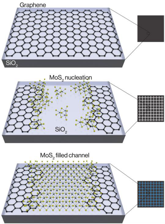
This schematic shows the chemical assembly of two-dimensional crystals. Graphene is first etched into channels and the TMDC molybdenum disulfide (MoS2) begins to nucleate around the edges and within the channel. On the edges, MoS2 slightly overlaps on top of the graphene. Finally, further growth results in MoS2 completely filling the channels. (credit: Berkeley Lab)
In an advance that helps pave the way for next-generation electronics and computing technologies — and possibly paper-thin devices — scientists with the U.S. Department of Energy’s Lawrence Berkeley National Laboratory (Berkeley Lab) have developed a way to chemically assemble transistors and circuits that are only a few atoms thick.
In addition, their method yields functional structures at a scale large enough to begin thinking about real-world applications and commercial scalability.
They reported their research online July 11 in the journal Nature Nanotechnology.
The scientists controlled the synthesis of a transistor in which narrow channels were etched onto conducting graphene, and a semiconducting material called a transition-metal dichalcogenide (TMDC) was seeded in the blank channels.
Both of these materials are single-layered crystals and atomically thin, so the two-part assembly yielded electronic structures that are essentially two-dimensional, and cover an area a few centimeters long and a few millimeters wide.
“This is a big step toward a scalable and repeatable way to build atomically thin electronics or pack more computing power in a smaller area,” says Xiang Zhang, a senior scientist in Berkeley Lab’s Materials Sciences Division who led the study.
Their work is part of a new wave of research aimed at keeping pace with Moore’s Law, which holds that the number of transistors in an integrated circuit doubles approximately every two years. To keep this pace, scientists predict that integrated electronics will soon require transistors that measure less than ten nanometers in length.
“With silicon, this will be extremely challenging, because the thickness of the transistor’s channel will become greater than the channel length, ultimately leading to difficult electrostatic control via the transistor gate,” the authors note. Nanomaterials such as inorganic nanowires and Stanford/IBM’s carbon nanotubes have been proposed, but require impractical “precise placement and orientation using complex fabrication techniques,” the authors point out.
The two-dimensional solution for keeping up with Moore’s law

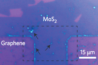
Optical image of the atomically thin graphene–MoS heterostructure. Arrows indicate nucleation (junctions) with graphene of the MoS2 areas, forming transistors. (credit: Mervin Zhao et al./Nature Nanotechnology)
So researchers have now looked to two-dimensional crystals that are only one molecule thick as alternative materials to keep up with Moore’s Law. Using that approach, the Berkeley Lab scientists developed a way to seed a single-layered semiconductor — in this case, the TMDC molybdenum disulfide (MoS2) — into channels lithographically etched within a sheet of conducting graphene. The two atomic sheets meet to form nanometer-scale junctions that make atomically thin transistors in which the graphene conductor efficiently injects current into the MoS2.
“This approach allows for the chemical assembly of electronic circuits, using two-dimensional materials, which show improved performance compared to using traditional metals to inject current into TMDCs,” says Mervin Zhao, a lead author and Ph.D. student in Zhang’s group at Berkeley Lab and UC Berkeley.
The scientists demonstrated the usefulness of the structure by assembling it into the logic circuitry of an inverter (NOT gate). This further underscores the technology’s ability to lay the foundation for a chemically assembled atomic computer, the scientists say. They also note that the two-dimensional crystals were synthesized at a wafer scale, so the scalable design is compatible with current semiconductor manufacturing.
The research was supported by the Office of Naval Research and the National Science Foundation. Scientists from Cornell University were also involved in the research.
Abstract of Large-scale chemical assembly of atomically thin transistors and circuits
Next-generation electronics calls for new materials beyond silicon, aiming at increased functionality, performance and scaling in integrated circuits. In this respect, two-dimensional gapless graphene and semiconducting transition-metal dichalcogenides have emerged as promising candidates due to their atomic thickness and chemical stability. However, difficulties with precise spatial control during their assembly currently impede actual integration into devices. Here, we report on the large-scale, spatially controlled synthesis of heterostructures made of single-layer semiconducting molybdenum disulfide contacting conductive graphene. Transmission electron microscopy studies reveal that the single-layer molybdenum disulfide nucleates at the graphene edges. We demonstrate that such chemically assembled atomic transistors exhibit high transconductance (10 µS), on–off ratio (∼106) and mobility (∼17 cm2 V−1 s−1). The precise site selectivity from atomically thin conducting and semiconducting crystals enables us to exploit these heterostructures to assemble two-dimensional logic circuits, such as an NMOS inverter with high voltage gain (up to 70).